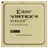
XC4VLX25-11FFG668C Xilinx Inc, XC4VLX25-11FFG668C Datasheet - Page 7

XC4VLX25-11FFG668C
Manufacturer Part Number
XC4VLX25-11FFG668C
Description
IC FPGA VIRTEX-4 24K 668-FCBGA
Manufacturer
Xilinx Inc
Series
Virtex™-4r
Specifications of XC4VLX25-11FFG668C
Number Of Logic Elements/cells
24192
Number Of Labs/clbs
2688
Total Ram Bits
1327104
Number Of I /o
448
Voltage - Supply
1.14 V ~ 1.26 V
Mounting Type
Surface Mount
Operating Temperature
0°C ~ 85°C
Package / Case
668-BBGA, FCBGA
Package
668FCBGA
Family Name
Virtex®-4
Device Logic Units
24192
Typical Operating Supply Voltage
1.2 V
Maximum Number Of User I/os
448
Ram Bits
1327104
For Use With
807-1004 - DAUGHTER CARD WITH VIRTEX-4HW-AFX-FF668-400 - BOARD DEV VIRTEX 4 FF668122-1523 - EVALUATION PLATFORM VIRTEX-4
Lead Free Status / RoHS Status
Lead free / RoHS Compliant
Number Of Gates
-
Other names
122-1490
Available stocks
Company
Part Number
Manufacturer
Quantity
Price
Company:
Part Number:
XC4VLX25-11FFG668C
Manufacturer:
XILINX
Quantity:
101
Company:
Part Number:
XC4VLX25-11FFG668C
Manufacturer:
Xilinx Inc
Quantity:
10 000
Part Number:
XC4VLX25-11FFG668C
Manufacturer:
XILINX/赛灵思
Quantity:
20 000
Power-On Power Supply Requirements
Xilinx® FPGAs require a certain amount of supply current
during power-on to insure proper device initialization. The
actual current consumed depends on the power-on ramp
rate of the power supply.
The power supplies can be turned on in any sequence,
though the specifications shown in
ommended power-on sequence of V
Xilinx does not specify the current for other power-on
sequences.
Table 5: Power-On Current for Virtex-4 Devices
Table 6: Power Supply Ramp Time
DS302 (v3.7) September 9, 2009
Product Specification
Notes:
1.
2.
XC4VLX15
XC4VLX25
XC4VLX40
XC4VLX60
XC4VLX80
XC4VLX100
XC4VLX160
XC4VLX200
XC4VSX25
XC4VSX35
XC4VSX55
XC4VFX12
XC4VFX20
XC4VFX40
XC4VFX60
XC4VFX100
XC4VFX140
V
V
V
CCINT
CCO
CCAUX
Symbol
Device
Typical values are specified at nominal voltage, 25°C.
Maximum values are specified under worst-case process, voltage, and temperature conditions.
Internal supply voltage relative to GND
Output drivers supply voltage relative to GND
Auxiliary supply voltage relative to GND
Typ
110
160
250
300
400
500
700
850
175
250
400
111
151
244
339
511
702
(1)
I
CCINTMIN
Max
1350
1500
1925
2550
3200
3700
3850
1350
2225
1100
1650
2250
3300
4250
Table 5
750
725
750
CCINT
(2)
, V
are for the rec-
Description
CCAUX
Typ
, V
110
225
280
335
500
500
110
165
225
167
222
278
500
60
85
56
56
www.xilinx.com
(1)
CCO
I
CCAUXMIN
Virtex-4 FPGA Data Sheet: DC and Switching Characteristics
.
Table 5
devices for proper power-on and configuration.
If the current minimums shown in
device powers on properly after all three supplies have
passed through their power-on reset threshold voltages.
Once initialized and configured, use the XPower tool to esti-
mate current drain on these supplies.
Max
100
125
150
300
350
425
600
600
150
200
300
100
100
250
350
500
825
(2)
shows the minimum current required by Virtex-4
Typ
150
150
200
250
250
100
150
125
150
200
250
50
75
75
75
50
75
(1)
I
CCOMIN
Ramp Time
0.20 to 50.0
0.20 to 50.0
0.20 to 50.0
Max
100
105
250
275
300
400
400
105
150
225
125
225
275
300
375
75
75
Table 5
(2)
are met, the
Units
Units
mA
mA
mA
mA
mA
mA
mA
mA
mA
mA
mA
mA
mA
mA
mA
mA
mA
ms
ms
ms
7


