MOD5282-100 NetBurner Inc, MOD5282-100 Datasheet - Page 5
MOD5282-100
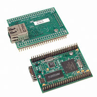
Manufacturer Part Number
MOD5282-100
Description
PROCESSOR MODULE 512KB FLASH
Manufacturer
NetBurner Inc
Datasheet
1.MOD5282-100IR.pdf
(5 pages)
Specifications of MOD5282-100
Module/board Type
Processor Module
For Use With/related Products
MOD5282
Lead Free Status / RoHS Status
Contains lead / RoHS non-compliant
Other names
528-1005


Table 2: NetBurner MOD5282 Pinout and Signal Descriptions
Pin
10
11
12
13
14
15
16
17
18
19
20
21
22
23
24
25
26
27
28
29
30
31
32
33
34
35
36
37
38
39
40
41
42
43
44
45
46
47
48
49
50
+
+
+
+
+
+
+
+
+
+
+
+
1
2
3
4
5
6
7
8
9
1
1
1
1
1
1
1
1
1
1
1
1
e t B u r n e r
CPU Pin
Networking in 1 Day!
N13
N12
G14
G13
D16
D15
C16
C14
T13
T12
R13
R12
P13
P12
F14
F16
F13
K14
F15
K15
K13
K16
E14
F16
E15
E13
B15
J14
J15
J13
J13
N6
T7
R1
R2
T2
R3
T3
T4
R4
P3
R7
P7
SPI_DOUT
Function
IRQ1_LVS
IRQ1_FET
IRQ3_LVS
IRQ3_FET
IRQ5_LVS
IRQ5_FET
IRQ7_LVS
IRQ7_FET
DTOUT3
DTOUT2
DTOUT1
DTOUT0
SPI_CLK
SPI_CS3
SPI_DIN
SPI_CS0
SPI_CS2
SPI_CS1
ADVCC
CANRX
URXD0
UTXD0
URXD1
UTXD1
CANTX
VCC3V
GPTA3
GPTB3
GPTA2
GPTB2
GPTA1
GPTB1
GPTA0
GPTB0
VCC3V
AN56
AN53
AN52
AN55
GND
GND
TIN2
TIN0
TIN1
TIN3
GND
GND
AN3
AN1
AN2
AN0
SDA
SCL
J2 Connector
Alt. Func.
IRQ1_RET
IRQ1_FRT
IRQ1_RET
IRQ1_FRT
IRQ5_RET
IRQ5_FRT
IRQ7_LVS
IRQ7_FET
URXD2
URXD2
UTXD2
UCTS0
UCTS1
UCTS0
UCTS1
URTS0
URTS1
UCTS0
UCTS1
URTS0
URTS1
UCTS0
UCTS1
URTS0
URTS1
URTS0
URTS1
Revision 1.0, April 4, 2006. © 2006 NetBurner, Inc. Specifications are subject to change without notice. Every effort
has been made to ensure all information is correct, but NetBurner, Inc. is not responsible for inadvertant errors.
Freescale(tm) and the Freescale logo are trademarks of Freescale Semiconductor, Inc. All other product or service
names are the property of their respective owners. (c) Freescale Semiconductor, Inc. 2006
GPIO
•
•
•
•
•
•
•
•
•
•
•
•
•
•
•
•
•
•
•
•
•
•
•
•
•
•
•
•
•
•
•
•
•
•
•
•
•
•
•
•
•
•
•
Description
Ground
Input power 3.3V
UART 0 Receive
UART 0 Transmit
ADVCC
Analog I/O CH3
Analog I/O CH1
Analog I/O CH2
Analog I/O CH56
Analog I/O CH0
Analog I/O CH53
Analog I/O CH52
Analog I/O CH55
Ground
General Purpose Timer A3
General Purpose Timer B3
General Purpose Timer A2
General Purpose Timer B2
General Purpose Timer A1
General Purpose Timer B1
UART 1 Receive
UART 1 Transmit
General Purpose Timer A0
General Purpose Timer B0
QSPI Clock
QSPI Chip Select 3
QSPI Input
QSPI Data Out
DMA Timer 2
UART 1 Clear to Send
QSPI Chip Select 0
DMA Timer 0
UART 1 Clear to Send
DMA Timer 3 Out or UART 0 Request to Send
UART 1 Request to Send
DMA Timer 2 Out or UART 0 Clear to Send
UART 1 Clear to Send
DMA Timer 1 Out or or UART 0 Request to Send
UART 1 Request to Send
QSPI Chip Select 2
DMA Timer 0 Out or UART 0 Clear to Send
UART 1 Clear to Send
DMA Timer 1
UART 1 Request to Send
DMA Timer 3
UART 1 Request to Send
I
QSPI Chip Select 1
CAN Receive or UART 2 Receive
I
IRQ1 Level-Sensitive, Rising Edge Triggered,
Falling Edge Triggered, Falling and Rising Edge Triggered
CAN Transmit
IRQ3 Level-Sensitive, Rising Edge Triggered,
Falling Edge Triggered, Falling and Rising Edge Triggered
Ground
IRQ5 Level-Sensitive, Rising Edge Triggered,
Falling Edge Triggered, Falling and Rising Edge Triggered
IRQ5 Level-Sensitive, Rising Edge Triggered,
Falling Edge Triggered, Falling and Rising Edge Triggered
Ground
Input power 3.3V
2
2
C Data Line
C Clock Line
2
4
4
4
4
2
or UART 2 Receive
In or UART 0 Clear to Send
In or UART 0 Clear to Send
In or UART 0 Request to Send
In or UART 0 Request to Send
or UART 2 Transmit
4
4
4
4
4
4
4
4
(1)
for J2 Connector
4
4
4
4
3,4
3,4
3,4
4
4
or
or
4
4
or
or
4
4
or
or
4
or
www.NetBurner.com NetBurner Datasheet MOD5282-B
4
or
Note:
1. Plus sign (+) denotes additional
alternate pin function
2. If using I
pull-up resistors to SDA/SCL.
3. The third UART ( UART2) can be
routed to either of the two pin
configurations: replacing CAN RX
andTX, or I2C SDA and SDL.
4.TIN0, TIN1 and TIN2 can be used as
external baud rate clocks for UART0,
UART1 and UART2
MOD5282
2
C, the module must add
Related parts for MOD5282-100
Image
Part Number
Description
Manufacturer
Datasheet
Request
R

Part Number:
Description:
PROCESSOR MODULE 512KB FLASH
Manufacturer:
NetBurner Inc
Datasheet:

Part Number:
Description:
Ethernet Modules & Development Tools 32Bit 66MHz Core Module 50Pin DIP
Manufacturer:
NetBurner Inc
Datasheet:
Part Number:
Description:
MCU, MPU & DSP Development Tools MOD5282 Core Module Development Kit
Manufacturer:
NetBurner Inc
Datasheet:

Part Number:
Description:
BOARD SERIAL-ETHERNET 512K FLASH
Manufacturer:
NetBurner Inc
Datasheet:

Part Number:
Description:
PROCESSOR MODULE FLASH MOD5272
Manufacturer:
NetBurner Inc
Datasheet:

Part Number:
Description:
DUAL PORT SERIAL-ETHERNET
Manufacturer:
NetBurner Inc
Datasheet:

Part Number:
Description:
PROCESSOR MODULE FLASH
Manufacturer:
NetBurner Inc
Datasheet:

Part Number:
Description:
MOD5234 10/100 ETHERNET MODULE
Manufacturer:
NetBurner Inc
Datasheet:

Part Number:
Description:
KIT DEVELOP NETWORK FOR MOD5282
Manufacturer:
NetBurner Inc
Datasheet:

Part Number:
Description:
KIT DEVELOP NETWORK FOR MOD5272
Manufacturer:
NetBurner Inc
Datasheet:

Part Number:
Description:
DUAL PORT SERIAL-ETHERNET
Manufacturer:
NetBurner Inc
Datasheet:

Part Number:
Description:
Ethernet Modules & Development Tools 32 Bit 66MHz 40 Pin DIP Industrial Temp
Manufacturer:
NetBurner Inc
Datasheet:

Part Number:
Description:
Ethernet ICs 32bit 147MHz CAN-to- Ethnt Device IndTemp
Manufacturer:
NetBurner Inc
Datasheet: