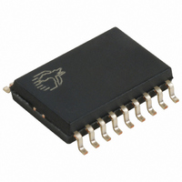
CY7C63723-SC Cypress Semiconductor Corp, CY7C63723-SC Datasheet - Page 33

CY7C63723-SC
Manufacturer Part Number
CY7C63723-SC
Description
IC MCU 8K LS USB/PS-2 18-SOIC
Manufacturer
Cypress Semiconductor Corp
Series
enCoRe™r
Specifications of CY7C63723-SC
Applications
USB Microcontroller
Core Processor
M8B
Program Memory Type
OTP (8 kB)
Controller Series
CY7C637xx
Ram Size
256 x 8
Interface
PS2, USB
Number Of I /o
10
Voltage - Supply
4 V ~ 5.5 V
Operating Temperature
0°C ~ 70°C
Mounting Type
Surface Mount
Package / Case
18-SOIC (7.5mm Width)
Lead Free Status / RoHS Status
Contains lead / RoHS non-compliant
Other names
428-1323
Available stocks
Company
Part Number
Manufacturer
Quantity
Price
Company:
Part Number:
CY7C63723-SC
Manufacturer:
CYPRESS
Quantity:
3 100
Company:
Part Number:
CY7C63723-SC
Manufacturer:
FUJI
Quantity:
154
Part Number:
CY7C63723-SC
Manufacturer:
CYPRESS/赛普拉斯
Quantity:
20 000
Figure 37. Port 0 Interrupt Enable Register (Address 0x04)
Bit [7:0]: P0 [7:0] Interrupt Enable
Figure 38. Port 1 Interrupt Enable Register
(Address 0x05)
Document #: 38-08022 Rev. *D
Read/Write
Read/Write
Bit Name
Bit Name
1 = Enables GPIO interrupts from the corresponding input pin.
0 = Disables GPIO interrupts from the corresponding input
pin.
Reset
Reset
Bit #
Bit #
Int
Wake-up
USB-
PS/2
Int
EP2
Int
1
1
1
W
W
7
0
7
0
D
D
CLK
CLK
CLK
D
CLR
CLR
CLR
W
W
6
0
6
0
Q
Q
Q
W
W
P0 Interrupt Enable
P1 Interrupt Enable
5
0
5
0
(Reg 0x21)
Enable [2]
(Reg 0x20)
(Reg 0x20)
Enable [0]
Enable [7]
W
W
4
0
4
0
Figure 36. Interrupt Controller Logic Block Diagram
W
W
3
0
3
0
W
W
2
0
2
0
W
W
1
0
1
0
SPI IRQ
Capture A IRQ
Capture B IRQ
USB-PS/2 IRQ
128-μs CLR
128-μs IRQ
1-ms CLR
1-ms IRQ
EP1 IRQ
EP2 CLR
EP2 IRQ
SPI CLR
Capture A CLR
Capture B CLR
GPIO CLR
GPIO IRQ
EP0 CLR
EP0 IRQ
EP1 CLR
Wake-up CLR
USB-PS/2 Clear
Wake-up IRQ
W
W
0
0
0
0
Interrupt
Encoder
Priority
Bit [7:0]: P1 [7:0] Interrupt Enable
The polarity that triggers an interrupt is controlled independently
for each GPIO pin by the GPIO Interrupt Polarity Registers.
Figure 39 and Figure control the interrupt polarity of each GPIO
pin.
Figure 39. Port 0 Interrupt Polarity Register
(Address 0x06)
Bit [7:0]: P0[7:0] Interrupt Polarity
Read/Write
Bit Name
1 = Enables GPIO interrupts from the corresponding input pin.
0 = Disables GPIO interrupts from the corresponding input
pin.
1 = Rising GPIO edge
0 = Falling GPIO edge
Reset
Bit #
Interrupt
IRQout
Vector
W
7
0
Acknowledge
CPU
To CPU
Interrupt
Interrupt
Enable
W
Global
6
0
CLR
Bit
P0 Interrupt Polarity
W
5
0
Controlled by DI, EI, and
RETI Instructions
W
4
0
IRQ Pending
W
(Bit 7, Reg 0xFF)
3
0
Int Enable
Sense
(Bit 2, Reg 0xFF)
CY7C63722C
CY7C63723C
CY7C63743C
W
2
0
IRQ
Page 33 of 53
W
1
0
W
0
0
[+] Feedback


