CY7C53120E4-40SXI Cypress Semiconductor Corp, CY7C53120E4-40SXI Datasheet - Page 10
CY7C53120E4-40SXI
Manufacturer Part Number
CY7C53120E4-40SXI
Description
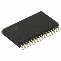
IC PROCESSOR NEURON 32-SOIC
Manufacturer
Cypress Semiconductor Corp
Series
Neuron®r
Datasheet
1.CY7C53150-20AXI.pdf
(16 pages)
Specifications of CY7C53120E4-40SXI
Package / Case
32-SOIC (11.30mm Width)
Applications
Network Processor
Core Processor
Pipelined
Program Memory Type
FLASH (4 kB), ROM (12 kB)
Controller Series
CY7C531xx
Ram Size
2K x 8
Interface
Serial
Number Of I /o
11
Voltage - Supply
4.5 V ~ 5.5 V
Operating Temperature
-40°C ~ 85°C
Mounting Type
Surface Mount
Product
Network Processor
Frequency
40 MHz
Maximum Operating Temperature
+ 85 C
Minimum Operating Temperature
- 40 C
Mounting Style
SMD/SMT
Core Operating Frequency
40MHz
Operating Supply Voltage (typ)
5V
Operating Supply Voltage (max)
5.5V
Operating Supply Voltage (min)
4.5V
Mounting
Surface Mount
Operating Temperature (max)
85C
Operating Temperature (min)
-40C
Operating Temperature Classification
Industrial
Core Size
8 Bit
No. Of I/o's
11
Program Memory Size
16KB
Ram Memory Size
2KB
Cpu Speed
40MHz
No. Of Timers
2
Embedded Interface Type
SCI
Digital Ic Case Style
SOIC
Rohs Compliant
Yes
Lead Free Status / RoHS Status
Lead free / RoHS Compliant
Lead Free Status / RoHS Status
Lead free / RoHS Compliant, Lead free / RoHS Compliant
Available stocks
Company
Part Number
Manufacturer
Quantity
Price
Company:

Part Number:
CY7C53120E4-40SXI
Manufacturer:
CYPRESS
Quantity:
190


Document #: 38-10001 Rev. *G
20 pF Load
30 pF Load
30 pF Load
30 pF Load
(A0 – A15)
Data (Out)
(D0 – D7)
(D0 – D7)
Address
Data (In)
R/W
E
Figure 6. Drive Levels and Test Point Levels for Timing Specifications Unless Otherwise Specified
t
AD
PW
Memory READ
EH
t
RD
Figure 7. Test Point Levels for Driven-to-Three-State Time Measurements
t
cyc
Figure 8. Signal Loading for Driven-to-Three-State Time Measurements
Address
PW
Data In
DRIVE TO 2.4V
DRIVE TO 0.4V
t
EL
DSR
A — Signal valid-to-signal valid specification (maximum or minimum)
B — Signal valid-to-signal invalid specification (maximum or minimum)
Figure 9. External Memory Interface Timing Diagram
TEST SIGNAL
t
AD
t
DHR
t
AH
Memory READ
V
V
C
OH
OL
L
– Measured low output drive level
= 30 pF
– Measured high output drive level
Address
Data In
t
t
DHR
DSR
2.0V
0.8V
B
V
A
V
I
LOAD
OH
OL
+ 0.5 V
– 0.5 V
= 1.4 mA
t
2.0V
0.8V
AD
Memory WRITE
t
t
t
AH
RH
DHZ
V
t
DDW
DD
t
WR
/2
Address
t
DHW
Data Out
CY7C53150, CY7C53120
t
DDZ
t
AD
Memory WRITE
t
AH
t
DDW
Address
t
DHZ
t
t
t
WH
DHW
AH
t
Data Out
DDZ
Page 10 of 16
[+] Feedback
Related parts for CY7C53120E4-40SXI
Image
Part Number
Description
Manufacturer
Datasheet
Request
R

Part Number:
Description:
Manufacturer:
Cypress Semiconductor Corp
Datasheet:
Part Number:
Description:
Manufacturer:
Cypress Semiconductor Corp
Datasheet:
Part Number:
Description:
Manufacturer:
Cypress Semiconductor Corp
Datasheet:
Part Number:
Description:
Manufacturer:
Cypress Semiconductor Corp
Datasheet:
Part Number:
Description:
Manufacturer:
Cypress Semiconductor Corp
Datasheet: