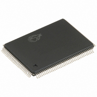
CY7C68013A-128AXI Cypress Semiconductor Corp, CY7C68013A-128AXI Datasheet - Page 52

CY7C68013A-128AXI
Manufacturer Part Number
CY7C68013A-128AXI
Description
IC MCU USB PERIPH HI SPD 128LQFP
Manufacturer
Cypress Semiconductor Corp
Series
EZ-USB FX2LP™r
Specifications of CY7C68013A-128AXI
Program Memory Type
ROMless
Package / Case
128-LQFP
Applications
USB Microcontroller
Core Processor
8051
Controller Series
CY7C680xx
Ram Size
16K x 8
Interface
I²C, USB, USART
Number Of I /o
40
Voltage - Supply
3 V ~ 3.6 V
Operating Temperature
-40°C ~ 85°C
Mounting Type
Surface Mount
Processor Series
CY7C68xx
Core
8051
Data Bus Width
8 bit
Data Ram Size
16 KB
Interface Type
I2C, USART, USB
Maximum Clock Frequency
48 MHz
Number Of Programmable I/os
40
Number Of Timers
3
Maximum Operating Temperature
+ 105 C
Mounting Style
SMD/SMT
Development Tools By Supplier
CY3684
Minimum Operating Temperature
- 40 C
Controller Family/series
(8051) USB
Core Size
8 Bit
No. Of I/o's
40
Program Memory Size
16KB
Cpu Speed
48MHz
No. Of Timers
3
Embedded Interface Type
I2C, USART, USB
Rohs Compliant
Yes
Lead Free Status / RoHS Status
Lead free / RoHS Compliant
For Use With
CY4611B - KIT USB TO ATA REFERENCE DESIGN428-1677 - KIT DEVELOPMENT EZ-USB FX2LP
Lead Free Status / Rohs Status
Lead free / RoHS Compliant
Other names
428-1943
CY7C68013A-128AXI
CY7C68013A-128AXI
Available stocks
Company
Part Number
Manufacturer
Quantity
Price
Company:
Part Number:
CY7C68013A-128AXI
Manufacturer:
EPCOS
Quantity:
43 000
Company:
Part Number:
CY7C68013A-128AXI
Manufacturer:
CY
Quantity:
5 530
Company:
Part Number:
CY7C68013A-128AXI
Manufacturer:
CY
Quantity:
6 100
Company:
Part Number:
CY7C68013A-128AXI
Manufacturer:
Cypress Semiconductor Corp
Quantity:
10 000
Figure 9-20
signals during a synchronous write using IFCLK as the
synchronizing clock. The diagram illustrates a single write
followed by burst write of 3 bytes and committing all 4 bytes as
a short packet using the PKTEND pin.
■
■
■
■
The same sequence of events are also shown for a burst write
and are marked with the time indicators of T = 0 through 5.
Note For the burst mode, SLWR and SLCS are left asserted for
the entire duration of writing all the required data values. In this
burst write mode, after the SLWR is asserted, the data on the
FIFO data bus is written to the FIFO on every rising edge of
IFCLK. The FIFO pointer is updated on each rising edge of
IFCLK. In
FIFO, SLWR is deasserted. The short 4 byte packet can be
committed to the host by asserting the PKTEND signal.
Document #: 38-08032 Rev. *T
At t = 0 the FIFO address is stable and the signal SLCS is
asserted. (SLCS may be tied low in some applications) Note
that t
running at 48 MHz, the FIFO address setup time is more than
one IFCLK cycle.
At t = 1, the external master/peripheral must outputs the data
value onto the data bus with a minimum set up time of t
before the rising edge of IFCLK.
At t = 2, SLWR is asserted. The SLWR must meet the setup
time of t
edge of IFCLK) and maintain a minimum hold time of t
from the IFCLK edge to the deassertion of the SLWR signal).
If the SLCS signal is used, it must be asserted with SLWR or
before SLWR is asserted (The SLCS and SLWR signals must
both be asserted to start a valid write condition).
While the SLWR is asserted, data is written to the FIFO and on
the rising edge of the IFCLK, the FIFO pointer is incremented.
The FIFO flag is also updated after a delay of t
rising edge of the clock.
SFA
SWR
Figure
has a minimum of 25 ns. This means when IFCLK is
shows the timing relationship of the SLAVE FIFO
(time from asserting the SLWR signal to the rising
9-20, after the four bytes are written to the
XFLG
WRH
from the
SFD
(time
There is no specific timing requirement that should be met for
asserting PKTEND signal with regards to asserting the SLWR
signal. PKTEND can be asserted with the last data value or
thereafter. The only requirement is that the setup time t
the hold time t
the number of data values committed includes the last value
written to the FIFO. In this example, both the data value and the
PKTEND signal are clocked on the same rising edge of IFCLK.
PKTEND can also be asserted in subsequent clock cycles. The
FIFOADDR lines should be held constant during the PKTEND
assertion.
Although there are no specific timing requirement for the
PKTEND assertion, there is a specific corner case condition that
needs attention while using the PKTEND to commit a one
byte/word packet. Additional timing requirements exists when
the FIFO is configured to operate in auto mode and it is desired
to send two packets: a full packet (full defined as the number of
bytes in the FIFO meeting the level set in AUTOINLEN register)
committed automatically followed by a short one byte or word
packet committed manually using the PKTEND pin.
In this case, the external master must ensure to assert the
PKTEND pin at least one clock cycle after the rising edge that
caused the last byte or word that needs to be clocked into the
previous auto committed packet (the packet with the number of
bytes equal to what is set in the AUTOINLEN register). Refer to
Figure 9-12 on page 48
PEH
CY7C68013A, CY7C68014A
CY7C68015A, CY7C68016A
must be met. In the scenario of
for further details on this timing.
Page 52 of 67
Figure
SPE
9-20,
and
[+] Feedback


