CY7C63743-SXC Cypress Semiconductor Corp, CY7C63743-SXC Datasheet - Page 38
CY7C63743-SXC
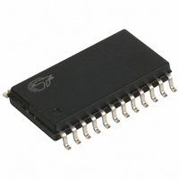
Manufacturer Part Number
CY7C63743-SXC
Description
IC MCU 8K USB/PS2 LS 24SOIC
Manufacturer
Cypress Semiconductor Corp
Series
enCoRe™r
Specifications of CY7C63743-SXC
Applications
USB Microcontroller
Core Processor
M8B
Program Memory Type
OTP (8 kB)
Controller Series
CY7C637xx
Ram Size
256 x 8
Interface
PS2, USB
Number Of I /o
16
Voltage - Supply
4 V ~ 5.5 V
Operating Temperature
0°C ~ 70°C
Mounting Type
Surface Mount
Package / Case
24-SOIC (7.5mm Width)
Lead Free Status / RoHS Status
Lead free / RoHS Compliant
Other names
428-1622
Available stocks
Company
Part Number
Manufacturer
Quantity
Price

Part Number:
CY7C63743-SXC
Manufacturer:
CYPRESS/赛普拉斯
Quantity:
20 000


24.0
Storage Temperature ..........................................................................................................................................–65°C to +150°C
Ambient Temperature with Power Applied ...............................................................................................................–0°C to +70°C
Supply Voltage on V
DC Input Voltage........................................................................................................................................... –0.5V to +V
DC Voltage Applied to Outputs in High Z State............................................................................................ –0.5V to + V
Maximum Total Sink Output Current into Port 0 and 1 and Pins.......................................................................................... 70 mA
Maximum Total Source Output Current into Port 0 and 1 and Pins ..................................................................................... 30 mA
Maximum On-chip Power Dissipation on any GPIO Pin ......................................................................................................50 mW
Power Dissipation ..............................................................................................................................................................300 mW
Static Discharge Voltage .................................................................................................................................................. > 2000V
Latch-up Current ........................................................................................................................................................... > 200 mA
25.0
Document #: 38-08022 Rev. *B
V
V
I
I
I
I
V
T
I
I
I
V
t
V
C
V
Notes:
10. In suspend mode, V
CC1
CC2
SB1
SB2
IL
SNK
SRC
VCCS
4.
5.
6.
7.
8.
9.
RSNTR
CC1
CC2
PP
LVR
REG
OHU
REG
Full functionality is guaranteed in V
Bench measurements taken under nominal operating conditions. Spec cannot be guaranteed at final test.
Total current cumulative across all Port pins, limited to minimize Power and Ground-Drop noise effects.
LVR is automatically disabled during suspend mode.
LVR will re-occur whenever V
V
output is not regulated, and should not be used as a general source of regulated voltage in that case. During receive of USB data, the VREG output drops
when D– is LOW due to internal series resistance of approximately 200 Ω at the VREG pin.
REG
specified for regulator enabled, idle conditions (i.e., no USB traffic), with load resistors listed. During USB transmits from the internal SIE, the VREG
Absolute Maximum Ratings
DC Characteristics
Operating Voltage
Operating Voltage
V
Oscillator Mode
Typical I
V
Oscillator Mode
Typical I
Standby Current – No Wake-up Osc
Standby Current – With Wake-up Osc
Programming Voltage (disabled)
Resonator Start-up Interval
Input Leakage Current
Max I
Max I
Low-Voltage Reset Trip Voltage
V
VREG Regulator Output Voltage
Capacitance on VREG Pin
Static Output High, driven
CC
CC
CC
Low-Voltage and Power-on Reset
Operating Supply Current – Internal
Operating Supply Current – External
Power-on Slew Time
SS
CC
CC
REG
CC1
CC2
GPIO Sink Current
GPIO Source Current
Relative to V
is only valid if R
= 13 mA
= 16 mA
USB Interface
CC
Parameter
drops below V
General
CC1
[5]
[5]
FOSC = 6 MHz; Operating Temperature = 0 to 70°C
range, except USB transmitter specifications and GPIO output currents are guaranteed for V
PU
SS
FOR
FOR
is connected from D– to VREG pin, and R
.................................................................................................................. –0.5V to +7.0V
LVR
. In suspend or with LVR disabled, BOR occurs whenever V
Note 4
Note 4
V
V
V
V
Oscillator off, D– > 2.7V
Oscillator off, D– > 2.7V
V
Any I/O pin
Cumulative across all ports
Cumulative across all ports
V
linear ramp: 0 to 4V
Load = R
External cap not required
R
CC
CC
CC
CC
CC
CC
PD
= 5.5V, no GPIO loading
= 5.0V. T = Room Temperature
= 5.5V, no GPIO loading
= 5.0V. T = Room Temperature
= 5.0V, ceramic resonator
below V
to Gnd
PU
[4]
+R
LVR
PD
Conditions
PD
is connected from D– to ground.
for >100 ns
[9, 10]
[8]
[6]
[6]
[7]
CC
drops below approximately 2.5V.
V
Min.
4.35
–0.4
3.5
3.0
2.8
LVR
CC2
CY7C63722
CY7C63723
CY7C63743
Max.
5.25
256
100
300
range.
5.5
0.4
4.0
3.6
3.6
20
17
25
75
70
30
1
Page 38 of 49
CC
CC
Unit
mA
mA
mA
mA
+0.5V
+0.5V
µA
µA
µA
ms
pF
µs
V
V
V
V
V
V
Related parts for CY7C63743-SXC
Image
Part Number
Description
Manufacturer
Datasheet
Request
R

Part Number:
Description:
Manufacturer:
Cypress Semiconductor Corp
Datasheet:
Part Number:
Description:
Manufacturer:
Cypress Semiconductor Corp
Datasheet:
Part Number:
Description:
Manufacturer:
Cypress Semiconductor Corp
Datasheet:
Part Number:
Description:
Manufacturer:
Cypress Semiconductor Corp
Datasheet:
Part Number:
Description:
Manufacturer:
Cypress Semiconductor Corp
Datasheet: