CY7C68013-56PVC Cypress Semiconductor Corp, CY7C68013-56PVC Datasheet - Page 18
CY7C68013-56PVC
Manufacturer Part Number
CY7C68013-56PVC
Description
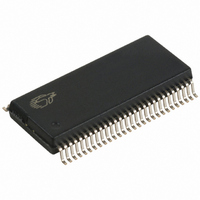
IC MCU USB PERIPH HI SPD 56SSOP
Manufacturer
Cypress Semiconductor Corp
Series
EZ-USB FX2LP™r
Datasheet
1.CY7C68013-56PVC.pdf
(52 pages)
Specifications of CY7C68013-56PVC
Applications
USB Microcontroller
Core Processor
8051
Program Memory Type
ROMless
Controller Series
CY7C680xx
Ram Size
16K x 8
Interface
I²C, USB, USART
Number Of I /o
24
Voltage - Supply
3 V ~ 3.6 V
Operating Temperature
0°C ~ 70°C
Mounting Type
Surface Mount
Package / Case
56-SSOP
Lead Free Status / RoHS Status
Contains lead / RoHS non-compliant
Other names
428-1332
Available stocks
Company
Part Number
Manufacturer
Quantity
Price
Company:

Part Number:
CY7C68013-56PVC
Manufacturer:
CY
Quantity:
5 530
Company:
Part Number:
CY7C68013-56PVC
Manufacturer:
CY
Quantity:
6 100
Part Number:
CY7C68013-56PVC
Manufacturer:
CYPRESS/赛普拉斯
Quantity:
20 000


Table 3-7. Strap Boot EEPROM Address Lines to These Values
3.17.2
At power-on reset the I
program/data. The available RAM spaces are 8 kbytes from 0x0000–0x1FFF and 512 bytes from 0xE000–0xE1FF. The 8051 will
be in reset. I
3.17.3
The 8051 can control peripherals connected to the I
compatible master control only, it is never an I
4.0
Figure 4-1 identifies all signals for the four package types. The following pages illustrate the individual pin diagrams, plus a
combination diagram showing which of the full set of signals are available in the 128-, 100-, and 56-pin packages.
The 56-pin package is the lowest-cost version. The signals on the left edge of the 56-pin package in Figure 4-1 are common to
all versions in the FX2 family. Three modes are available in all package versions: Port, GPIF master, and Slave FIFO. These
modes define the signals on the right edge of the diagram. The 8051 selects the interface mode using the IFCONFIG[1:0] register
bits. Port mode is the power-on default configuration.
The 100-pin package adds functionality to the 56-pin package by adding these pins:
The 128-pin package is the full version, adding the 8051 address and data buses plus control signals. Note that two of the required
signals, RD# and WR#, are present in the 100-pin version. In the 100-pin and 128-pin versions, an 8051 control bit can be set to
pulse the RD# and WR# pins when the 8051 reads from/writes to PORTC.
Note:
Document #: 38-08012 Rev. *C
4.
• PORTC or alternate GPIFADR[7...0] address signals
• PORTE or alternate GPIFADR8 address signals and 7 more 8051 signals
• 3 GPIF Control signals
• 4 GPIF Ready signals
• Nine 8051 signals (two USARTs, three timer inputs, INT4,and INT5#)
• BKPT, RD#, WR#
16
128
256
4K
8K
This EEPROM does not have address pins.
Bytes
I
I
2
2
Pin Assignments
C-compatible Interface Boot Load Access
C-compatible Interface General Purpose Access
2
C-compatible interface boot loads only occur after power-on reset.
2
C-compatible interface boot loader will load the VID/PID/DID/a configuration byte and up to 8 kbytes of
24LC00
24LC01
24LC02
24LC32
24LC64
[4]
Example EEPROM
2
C-compatible slave.
2
C-compatible bus using the I2CTL and I2DAT registers. FX2 provides I
N/A
A2
0
0
0
0
N/A
A1
0
0
0
0
CY7C68013
Page 18 of 52
N/A
A0
0
0
1
1
2
C
Related parts for CY7C68013-56PVC
Image
Part Number
Description
Manufacturer
Datasheet
Request
R

Part Number:
Description:
IC MCU USB PERIPH HI SPD 100LQFP
Manufacturer:
Cypress Semiconductor Corp
Datasheet:

Part Number:
Description:
IC MCU USB PERIPH HI SPD 56SSOP
Manufacturer:
Cypress Semiconductor Corp
Datasheet:
Part Number:
Description:
IC MCU USB PERIPH HI SPD 100LQFP
Manufacturer:
Cypress Semiconductor Corp
Datasheet:

Part Number:
Description:
Manufacturer:
Cypress Semiconductor Corp
Datasheet:
Part Number:
Description:
Manufacturer:
Cypress Semiconductor Corp
Datasheet:

Part Number:
Description:
Manufacturer:
Cypress Semiconductor Corp
Datasheet:
Part Number:
Description:
Manufacturer:
Cypress Semiconductor Corp
Datasheet:
Part Number:
Description:
Manufacturer:
Cypress Semiconductor Corp
Datasheet:
Part Number:
Description:
Manufacturer:
Cypress Semiconductor Corp
Datasheet: