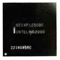
GCIXP1250BC Intel, GCIXP1250BC Datasheet - Page 21

GCIXP1250BC
Manufacturer Part Number
GCIXP1250BC
Description
IC MPU NETWORK 232MHZ 520-BGA
Manufacturer
Intel
Specifications of GCIXP1250BC
Rohs Status
RoHS non-compliant
Processor Type
Network
Features
32-bit StrongARM RISC Core
Speed
232MHz
Voltage
3.3V
Mounting Type
Surface Mount
Package / Case
520-BGA
Pin Count
520
Mounting
Surface Mount
Operating Temperature (max)
85C
Operating Temperature (min)
-40C
Operating Temperature Classification
Industrial
Lead Free Status / Rohs Status
Not Compliant
Other names
837414
Available stocks
Company
Part Number
Manufacturer
Quantity
Price
Company:
Part Number:
GCIXP1250BC
Manufacturer:
INTEL
Quantity:
77
Specification Changes
1.
2.
3.
4.
Specification Update
SRAM Bus Signal Timing Parameters
The maximum clock to data output valid delay (T
specified as 4.0 ns. The new T
The maximum clock to control outputs valid delay (T
originally specified as 4.0 ns. The new T
The minimum data input setup time before SCLK for pipelined SRAMs (T
operation was originally specified as 3.75 ns. The new T
SDRAM Bus Signal Timing Parameters
The maximum clock to data output valid delay (T
specified as 3.4 ns. The new T
The maximum SDCLK to control output valid delay (T
originally specified as 3.4 ns. The new T
T
originally specified as 3.75 ns. The new T
T
specified as 3.75 ns. The new T
FCLK AC Parameter Measurements
The parameter values for T
The minimum Clock high time (T
ns.
The minimum Clock low time (T
ns.
Both T
50% duty cycle and can vary worst case 45-55%”.
The units used for Clock rise (T
new unit is ns.
SRAM SCLK Signal AC Parameters
The minimum Cycle Time (T
new T
The minimum Cycle High Time (T
The new T
The minimum Cycle Low Time (T
The new T
sup
sup
, the minimum data input setup time before SDCLK value for 200 MHz operation was
, the minimum data input setup time before SDCLK for 232 MHz operation was originally
cyc
high
value is 8.62 ns.
high
low
and T
value 4.02 ns.
value is 4.02 ns.
low
have been further clarified by the statement “T
high
cyc
val
val
, T
sup
r
) for 232 MHz operation was originally specified as 8.6 ns. The
) and Clock fall (T
low
value is 3.35 ns.
value is 3.3 ns.
low
high
low
value is 3.70 ns.
high
) was originally specified as 4.5 ns. The new T
, and the T
) was originally specified as 4.5 ns. The new T
) for 232 MHz operation was originally specified as 4.6 ns.
) for 232 MHz operation was originally specified as 4.6 ns.
ctl
ctl
sup
value is 3.05 ns.
value is 2.90 ns.
value is 3.70 ns.
r
and T
val
val
f
) time was originally specified as V/ns. The
) value for 232 MHz operation was originally
) value for 232 MHz operation was originally
ctl
f
ctl
units have changed as follows:
) value for 232 MHz operation was
sup
) value for 232 MHz operation was
value is 3.10 ns.
Intel
®
high
IXP1250 Network Processor
and T
sup
Specification Changes
low
) value for 232 MHz
are based on a
high
high
value is 3.8
value is 3.8
21


