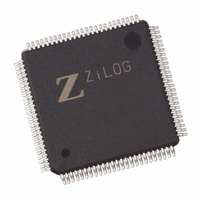
Z8018233ASC1838TR Zilog, Z8018233ASC1838TR Datasheet - Page 6

Z8018233ASC1838TR
Manufacturer Part Number
Z8018233ASC1838TR
Description
IC Z180 MPU 100VQFP
Manufacturer
Zilog
Datasheet
1.Z8018233FSG.pdf
(109 pages)
Specifications of Z8018233ASC1838TR
Processor Type
Z180
Features
Smart Peripheral Controller
Speed
33MHz
Voltage
5V
Mounting Type
Surface Mount
Package / Case
100-LQFP
Lead Free Status / RoHS Status
Contains lead / RoHS non-compliant
Available stocks
Company
Part Number
Manufacturer
Quantity
Price
Zilog
Z180 CPU SIGNALS (Continued)
/NMI. Non-maskable interrupt (input, negative edge
triggered). /NMI has a higher priority than /INT and is
always recognized at the end of an instruction, regardless
of the state of the interrupt enable flip-flops. This signal
forces CPU execution to continue at location 0066H.
/INT0. Maskable Interrupt Request 0 (input/output active
Low). This signal is generated by external I/O devices. The
CPU will honor this request at the end of the current
instruction cycle as long as the /NMI and /BUSREQ signals
are inactive. The CPU acknowledges this interrupt request
with an interrupt acknowledge cycle. During this cycle,
both the /M1 and /IORQ signals become active. The
internal Z180 MPU’s /INT0 source is: /INT0 or ESCC or the
MIMIC. This input is level triggered. /INT0 is an open-drain
output, so you can connect other open-drain interrupts
onto the circuit in addition to haveing a pull-up to VCC.
Z180 MPU UART AND SIO SIGNALS
CKA0, CKA1. Asynchronous Clocks 0 and 1 (bi-directional,
active High). These pins are the transmit and receive
clocks for the synchronous channels. CKA0 is multiplexed
with /DREQ0 on the CKA0//DREQ0 pin. CKA1 is multiplexed
with /TEND0 on the CKA1//TEND0 pin.
CKS. Serial Clock (bi-directional, active High). This line is
clock for the CSIO channel and is multiplexed with the
ESCC signal (/W//REQB) and the 16550 MIMIC interface
signal /HTxRDY on the CKS//W//REQB//HTxRDY pin.
/DCD0. Data Carrier Detect 0 (input, active Low). This is a
programmable modem control signal for ASCI channel 0.
/DCD0 is multiplexed with the PB2 (parallel Port B, bit 2) on
the /DCD0/PB2 pin.
/RTS0. Request to Send 0 (output, active Low). This is a
programmable modem control signal for ASCI channel 0.
This pin is multiplexed with PB0 (parallel Port B, bit 0) on the
/RTS0/PB0 pin.
/CTS0. Clear to Send 0 (input, active Low). This line is a
modem control signal for the ASCI channel 0. This pin is
multiplexed with PB1 (parallel Port B, bit 1) on the /CTS0
/PB1 pin.
3-6
PS009801-0301
P R E L I M I N A R Y
/INT1, /INT2. Maskable Interrupt Requests 1 and 2 (inputs,
active Low). This signal is generated by external I/O
devices. The CPU will honor these requests at the end of
the current instruction cycle as long as the /NMI, /BUSREQ,
and /INT0 signals are inactive. The CPU acknowledges
these interrupt requests with an interrupt acknowledge
cycle. Unlike the acknowledgment for /INT0, during this
cycle neither the /M1 or /IORQ signals become active.
These pins may be programmed to provide an active Low
level on rising or falling edge interrupts. The level of the
external /INT1 and /INT2 pins may be read through bits
PC6 and PC7 of parallel Port C. Pin /INT1/PC6 multiplexes
/INT1 and PC6. Pin /INT2/PC7 multiplexes /INT2 and PC7.
/RFSH. Refresh (input/output, active Low, tri-state).
Together with /MREQ, /RFSH indicates that the current
CPU machine cycle and the contents of the address bus
should be used for refresh of dynamic memories. The low
order 8 bits of the address bus (A7-A0) contain the refresh
address. This signal is analogous to the /REF signal of the
Z64180.
TxA0. Transmit Data 0 (output, active High). This signal is
the transmitted data from the ASCI channel 0. This pin is
multiplexed with PB3 (parallel Port B, bit 3) on the
TxA0/PB3 pin.
TxS. Clocked Serial Transmit Data (output, active High) .
This line is the transmitted data from the CSIO channel. TxS
is multiplexed with the ESCC signal (/DTR//REQB) and the
16550 MIMIC interface signal HINTR on the TxS//DTR
//REQB//HINTR pin.
RxA0. Receive Data 0 (input, active High). This signal is
the receive data to ASCI channel 0. This pin is multiplexed
with PB4 (parallel Port B, bit 4) on the RxA0/PB4.
RxS. Clocked Serial Receive Data (input, active High).
This line is the receive data for the CSIO channel. RxS is
multiplexed with the /CTS1 signal for ASCI channel 1 and
with PB7 (parallel Port B, bit 7) on the RxS//CTS1/PB7 pin.
RxA1. Received Data ASCI channel 1 (input, active High).
This pin is multiplexed with PB6 (parallel Port B, bit 6) on the
RxA1/PB6 pin.
TxA1. Transmitted Data ASCI Channel 1 (output, active
High). This pin is multiplexed with PB5 (parallel Port B, bit
5) on the TxA1/PB5 pin.
Z
ILOG
I
NTELLIGENT
DS971820600
Z80182/Z8L182
P
ERIPHERAL


