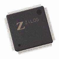
Z8018233ASG Zilog, Z8018233ASG Datasheet - Page 22

Z8018233ASG
Manufacturer Part Number
Z8018233ASG
Description
IC 33MHZ STATIC MIMIC 100-LQFP
Manufacturer
Zilog
Datasheet
1.Z8018233FSG.pdf
(109 pages)
Specifications of Z8018233ASG
Processor Type
Z180
Features
Smart Peripheral Controller
Speed
33MHz
Voltage
5V
Mounting Type
Surface Mount
Package / Case
100-LQFP
Processor Series
Z8018xx
Core
Z80
Data Bus Width
8 bit
Program Memory Type
ROMLess
Interface Type
UART
Maximum Clock Frequency
33 MHz
Number Of Programmable I/os
24
Number Of Timers
2
Operating Supply Voltage
4.5 V to 5.5 V
Maximum Operating Temperature
+ 70 C
Mounting Style
SMD/SMT
Minimum Operating Temperature
0 C
Lead Free Status / RoHS Status
Lead free / RoHS Compliant
Available stocks
Company
Part Number
Manufacturer
Quantity
Price
Zilog
16550 MIMIC FIFO DESCRIPTION
The receiver FIFO consists of a 16-word FIFO capable of
storing eight data bits and three error bits for each character
stored (Figure 7). Parity error, Framing error and Break
detect bits are stored along with the data bits by copying
their value from three shadow bits that are Write Only bits
for the Z80180 MPU LSR address. The three shadow bits
are cleared after they are copied to the FIFO memory. In
FIFO mode, to write error bits into the receiver FIFO, the
MPU must first write the Parity, Framing and Break detect
status to the Line Status Register (shadow bits) and then
write the character associated into the receiver buffer. The
data and error bits will then move into the same address in
3-22
MPU Side
Interface
MPU
CNTL
Line
MPU
Databus
(MPU Side Write)
MPU Write
LSR Shadow
B2-B4
Internal Clock
MPU
IRQ
Internal Clock
Sync
8
Figure 7. 16550 MIMIC Receiver FIFO Block Diagram
W
R
T
E
B
U
F
F
E
R
I
Pointer
Write
PS009801-0301
P R E L I M I N A R Y
Data Bits
16x8
ALU
the FIFO. The error bits become available to the PC side of
the interface when that particular location becomes the
next address to read (top of FIFO). At that time, they may
either be read by the PC by accessing them in the LSR, or
they may cause an interrupt to the PC interface if so
enabled. The error bits are set by the error status of the byte
at the top of the FIFO, but may only be cleared by reading
the LSR. If successive reads of the receiver FIFO are
performed without reading the LSR, the status bits will be
set if any of the bytes read have the respective error bit set.
See Table 6 for the setting and clearing of the Line Status
Register bits.
3
Pointer
16x3
Error
Bits
Read
error
3
R
E
A
D
B
U
F
F
E
R
Internal Clock
8
5
Sync
PC Read
LSR
B2-B4
Z
ILOG
I
NTELLIGENT
(PC Side Read)
DS971820600
FIFO Control
Z80182/Z8L182
Databus
Register
PC Side
MIMIC or
Interface
PC Side
Cntrl
16550
Line
P
PC
IRQ
ERIPHERAL
PC


