FWIXP425BB Intel, FWIXP425BB Datasheet - Page 4
FWIXP425BB
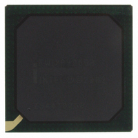
Manufacturer Part Number
FWIXP425BB
Description
IC NETWRK PROCESSR 266MHZ 492BGA
Manufacturer
Intel
Specifications of FWIXP425BB
Processor Type
Network
Features
XScale Core
Speed
266MHz
Voltage
1.3V
Mounting Type
Surface Mount
Package / Case
492-BGA
Lead Free Status / RoHS Status
Contains lead / RoHS non-compliant
Other names
852264
Available stocks
Company
Part Number
Manufacturer
Quantity
Price

Part Number:
FWIXP425BB
Manufacturer:
INTEL
Quantity:
20 000


Intel
Contents
5.0
4
®
Electrical Specifications ............................................................................................................. 74
5.1
5.2
5.3
5.4
5.5
5.6
5.7
5.8
IXP42X Product Line and IXC1100 Control Plane Processor
Absolute Maximum Ratings ................................................................................................ 74
V
5.2.1
5.2.2
5.2.3
5.2.4
RCOMP Pin Requirements................................................................................................. 77
DC Specifications ............................................................................................................... 77
5.4.1
5.4.2
5.4.3
5.4.4
5.4.5
5.4.6
5.4.7
5.4.8
5.4.9
5.4.10 High-Speed, Serial Interface 1 DC Parameters..................................................... 81
5.4.11 High-Speed and Console UART DC Parameters .................................................. 82
5.4.12 GPIO DC Parameters ............................................................................................ 83
5.4.13 JTAG DC Parameters............................................................................................ 83
5.4.14 Reset DC Parameters............................................................................................ 83
AC Specifications................................................................................................................ 84
5.5.1
5.5.2
5.5.3
Power Sequence .............................................................................................................. 111
I
Ordering Information......................................................................................................... 112
CC
CCPLL1
and Total Average Power ........................................................................................... 112
V
V
V
V
Operating Conditions ............................................................................................. 77
PCI DC Parameters ............................................................................................... 78
USB DC Parameters.............................................................................................. 78
UTOPIA-2 DC Parameters .................................................................................... 79
MII DC Parameters ................................................................................................ 79
MDIO DC Parameters............................................................................................ 80
SDRAM Bus DC Parameters................................................................................. 80
Expansion Bus DC Parameters ............................................................................. 81
High-Speed, Serial Interface 0 DC Parameters..................................................... 81
Clock Signal Timings ............................................................................................. 84
5.5.1.1
5.5.1.2
5.5.1.3
5.5.1.4
5.5.1.5
Bus Signal Timings ................................................................................................ 87
5.5.2.1
5.5.2.2
5.5.2.3
5.5.2.4
5.5.2.5
5.5.2.6
5.5.2.7
5.5.2.8
5.5.2.9
Reset Timings...................................................................................................... 110
, V
CCPLL1
CCPLL2
CCOSCP
CCOSC
CCPLL2
Requirement ............................................................................................ 76
Requirement ............................................................................................ 74
Requirement ............................................................................................ 75
, V
Requirement .......................................................................................... 75
Processor Clock Timings ....................................................................... 84
PCI Clock Timings ................................................................................. 86
MII Clock Timings .................................................................................. 86
UTOPIA-2 Clock Timings....................................................................... 86
Expansion Bus Clock Timings ............................................................... 86
PCI ......................................................................................................... 87
USB Interface......................................................................................... 88
UTOPIA-2 .............................................................................................. 89
MII .......................................................................................................... 90
MDIO...................................................................................................... 91
SDRAM Bus........................................................................................... 92
Expansion Bus ....................................................................................... 93
High-Speed, Serial Interfaces .............................................................. 107
JTAG.................................................................................................... 109
CCOSCP
, V
CCOSC
Pin Requirements .................................................. 74
Datasheet
Related parts for FWIXP425BB
Image
Part Number
Description
Manufacturer
Datasheet
Request
R

Part Number:
Description:
Microprocessor: Intel Celeron M Processor 320 and Ultra Low Voltage Intel Celeron M Processor at 600MHz
Manufacturer:
Intel Corporation
Part Number:
Description:
Intel 82550 Fast Ethernet Multifunction PCI/CardBus Controller
Manufacturer:
Intel Corporation
Datasheet:
Part Number:
Description:
Intel StrataFlash memory 32 Mbit. Access speed 120 ns
Manufacturer:
Intel Corporation
Datasheet:
Part Number:
Description:
Intel StrataFlash memory 32 Mbit. Access speed 120 ns
Manufacturer:
Intel Corporation
Datasheet:
Part Number:
Description:
Intel StrataFlash memory 64 Mbit. Access speed 150 ns
Manufacturer:
Intel Corporation
Datasheet:
Part Number:
Description:
Intel StrataFlash memory 32 Mbit. Access speed 100 ns
Manufacturer:
Intel Corporation
Datasheet:
Part Number:
Description:
DA28F640J5A-1505 Volt Intel StrataFlash Memory
Manufacturer:
Intel Corporation
Datasheet:
Part Number:
Description:
5 Volt Intel StrataFlash?? Memory
Manufacturer:
Intel Corporation
Datasheet:
Part Number:
Description:
5 Volt Intel StrataFlash?? Memory
Manufacturer:
Intel Corporation
Part Number:
Description:
Intel 6300ESB I/O Controller Hub
Manufacturer:
Intel Corporation
Datasheet:
Part Number:
Description:
Intel 82801DB I/O Controller Hub (ICH4), Pb-Free SLI
Manufacturer:
Intel Corporation
Datasheet:
Part Number:
Description:
Intel 82801FB I/O Controller Hub (ICH6)
Manufacturer:
Intel Corporation
Datasheet:
Part Number:
Description:
Intel Strataflash Memory28F128J3 28F640J3 28F320J3
Manufacturer:
Intel Corporation
Datasheet:
Part Number:
Description:
Controllers, Intel 430TX PCIset: 82439TX System Controller (MTXC)
Manufacturer:
Intel Corporation