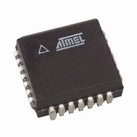
AT22LV10-25JI Atmel, AT22LV10-25JI Datasheet

AT22LV10-25JI
Specifications of AT22LV10-25JI
Available stocks
Related parts for AT22LV10-25JI
AT22LV10-25JI Summary of contents
Page 1
... All speed ranges are specified over the 3.0V to 5.5V range. All pins offer a low 10 µA leakage. The AT22LV10L provides the optimum low-power CMOS PLD solution, with low DC power (1 mA typical 3.3V) and full CMOS output levels. The AT22LV10L CC significantly reduces total system power, allowing battery powered operation ...
Page 2
... Full CMOS output levels help reduce power in many other system components. The AT22LV10 and AT22LV10L logic architectures are identical to the familiar 22V10. Each output is allocated from eight to 16 product terms, which allows highly complex logic functions to be realized. Two additional product terms are included to provide synchronous preset and asynchronous reset ...
Page 3
... V 4. 3.0V Com., Ind 4.5V Com., Ind 3.0V Com., Ind -100 µ 3.0V/4. -0.4 mA/-4 Max corresponds to 3.6V. CC AT22LV10(L) Min Typ Max Units 10 µA 10 µA 20/50 35/90 mA 20/50 45/100 mA 1/2 4/12 mA 1/2 5/15 mA -120 mA -0.6 0.8 -0.6 0.6 2 0.75 CC 0.5 0.5 ...
Page 4
... AC Characteristics for the AT22LV10 Symbol Parameter Input or Feedback to Non Registered Output t Input to Output Enable EA t Input to Output Disable ER t Clock to Feedback CF t Clock to Output CO t Input or Feedback Setup Time S t Hold Time H t Clock Period P t Clock Width W External Feedback 1/(t +t ...
Page 5
... AC Characteristics for the AT22LV10L Symbol Parameter t Input or Feedback to Non-Registered Output PD t Input to Output Enable EA t Input to Output Disable ER t Clock to Feedback CF t Clock to Output CO t Feedback Setup Time SF t Input Setup Time S t Hold Time H t Clock Period P t Clock Width ...
Page 6
... Functional Logic Diagram AT22LV10(L) AT22LV10(L) 6 ...
Page 7
... Note: 1. Typical values for nominal supply voltage. This parameter is only sampled and is not 100% tested. Erasure Characteristics The entire fuse array of an AT22LV10 or AT22LV10L is erased after exposure to ultraviolet light at a wavelength of 2537 Å. Complete erasure is assured after a minimum of 20 minutes exposure using 12,000 µW/cm spaced one inch away from the chip ...
Page 8
... AT22LV10(L) 8 ...
Page 9
... AT22LV10(L) 9 ...
Page 10
... Wide, Plastic Dual Inline Package OTP (PDIP) 24S 24-lead, 0.300" Wide, Plastic Gull-Wing Small Outline OTP (SOIC) AT22LV10(L) 10 Ordering Code AT22LV10-20JC AT22LV10-20PC AT22LV10-20SC AT22LV10-20JI AT22LV10-20PI AT22LV10-20SI AT22LV10-25JC AT22LV10-25PC AT22LV10-25SC AT22LV10-25JI AT22LV10-25PI AT22LV10-25SI AT22LV10L-25JC AT22LV10L-25PC AT22LV10L-25SC AT22LV10L-25JI AT22LV10L-25PI AT22LV10L-25SI Package Type Package Operation Range 28J Commercial 24P3 ...
Page 11
... SQ .043(1.09) .020(.508) .120(3.05) .090(2.29) .180(4.57) .165(4.19) .299(7.60) .420(10.7) .291(7.39) .393(9.98) .105(2.67) .092(2.34) .013(.330) .009(.229) AT22LV10(L) 1.27(32.3) 1.25(31.7) PIN 1 .090(2.29) 1.100(27.94) REF .200(5.06) .005(.127) MAX SEATING PLANE .070(1.78) .151(3.84) .020(.508) .125(3.18) .023(.584) ...
Page 12
... No licenses to patents or other intellectual prop- erty of Atmel are granted by the Company in connection with the sale of Atmel products, expressly or by implication. Atmel’s products are not authorized for use as critical components in life support devices or systems. ...


