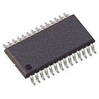
CS4272-DZZ Cirrus Logic Inc, CS4272-DZZ Datasheet - Page 8

CS4272-DZZ
Manufacturer Part Number
CS4272-DZZ
Description
IC CODEC 24BIT 114DB 28-TSSOP
Manufacturer
Cirrus Logic Inc
Type
Stereo Audior
Specifications of CS4272-DZZ
Data Interface
Serial
Resolution (bits)
24 b
Number Of Adcs / Dacs
2 / 2
Sigma Delta
Yes
Dynamic Range, Adcs / Dacs (db) Typ
114 / 114
Voltage - Supply, Analog
4.75 V ~ 5.25 V
Voltage - Supply, Digital
3.1 V ~ 5.25 V
Operating Temperature
-40°C ~ 85°C
Mounting Type
Surface Mount
Package / Case
28-TSSOP
Audio Codec Type
Stereo
No. Of Adcs
2
No. Of Dacs
2
No. Of Input Channels
3
No. Of Output Channels
3
Adc / Dac Resolution
24bit
Adcs / Dacs Signal To Noise Ratio
114dB
Lead Free Status / RoHS Status
Lead free / RoHS Compliant
For Use With
598-1004 - EVAL BOARD CS4272 STEREO CODEC
Lead Free Status / RoHS Status
Lead free / RoHS Compliant, Lead free / RoHS Compliant
Available stocks
Company
Part Number
Manufacturer
Quantity
Price
Part Number:
CS4272-DZZ
Manufacturer:
CIRRUS
Quantity:
20 000
Company:
Part Number:
CS4272-DZZR
Manufacturer:
TI
Quantity:
12
8
1.9
1.10 Power
1.11 Grounding and Power Supply Decoupling
The evaluation board has been designed to allow interfacing with external systems via the
headers J26, J32, J17, and J24.
The 10-pin header, J26, allows the user bidirectional access to MCLK, SCLK, and LRCK. The
direction of these signals is set using S1 (see Table 2 for switch control options) or the control
port GUI. Also accessible from this header is a buffered version of the SDOUT signal from
the CS4272, and a buffered input which, using S1 or the GUI, can be configured to drive the
CS4272 SDIN pin. Care should be taken to ensure that the crystal (Y2) is removed when the
board is configured to receive MCLK from this header.
The 2-pin header, J17, allows the user to supply the CS8406 with an external data source.
This option is available through the control port GUI and may be asserted by setting the
CS8406 data source to “Header”.
The 2-pin header, J24, supplies the user with a buffered version of the SDOUT signal gener-
ated by the CS8416. This may be used, for instance, to route received S/PDIF data off-board
for processing before introducing it at the SDIN position on J26.
The 6-pin header, J32, allows the user bidirectional access to the SPI/I
signals on J32 default to outputs. When a jumper is placed across J34, the header (J32) may
be used as an input. When set as an input, the control signals on J32 are routed to the cor-
responding control pins on the CS4272 and external control signals may be applied.
Power must be supplied to the evaluation board through at least three binding posts, +5.0 V
(J1), +18.0 V (J6), and -18.0 V (J7). Jumper J10 allows the user to connect the VA supply of
the CS4272 to a fixed +5.0 V supply or to another separate binding post (J5). Jumpers J8
and J9 connect the VL and VD supply, respectively, to a fixed +5.0 V or +3.3 V supply or to
two separate binding posts (J2 and J3) for variable voltage settings. All voltage inputs must
be referenced to the single black banana-type ground connector (see Figure 15).
It should be noted that devices other than the CS4272 are powered from the VL supply and
therefore VL must be limited to a minimum of 3.3 V.
WARNING:Please refer to the CS4272 data sheet for allowable voltage levels.
The CS4272 requires careful attention to power supply and grounding arrangements to opti-
mize performance. Figure 5 provides an overview of the connections to the CS4272,
Figure 16 shows the component placement, Figure 17 shows the top layout, and Figure 18
shows the bottom layout. The decoupling capacitors are located as close to the CS4272 as
possible. Extensive use of ground plane fill in the evaluation board yields large reductions in
radiated noise.
External Control Headers
2
C control signals. The
CDB4272


