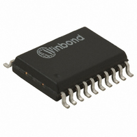
W681511SG TR Nuvoton Technology Corporation of America, W681511SG TR Datasheet - Page 8

W681511SG TR
Manufacturer Part Number
W681511SG TR
Description
IC VOICEBAND CODEC 5V 1CH 20SOP
Manufacturer
Nuvoton Technology Corporation of America
Type
PCMr
Datasheet
1.W681511SG_TR.pdf
(33 pages)
Specifications of W681511SG TR
Data Interface
PCM Audio Interface
Resolution (bits)
8 b
Number Of Adcs / Dacs
1 / 1
Sigma Delta
No
Voltage - Supply, Analog
4.5 V ~ 5.5 V
Voltage - Supply, Digital
4.5 V ~ 5.5 V
Operating Temperature
-40°C ~ 85°C
Mounting Type
Surface Mount
Package / Case
20-SOP
For Use With
W681513DK - KIT DEVELOPMENT FOR W681513W681512DK - KIT DEVELOPMENT FOR W681512W681511DK - KIT DEVELOPMENT FOR W681511W681512ES - EVALUATION SYSTEM FOR W681512
Lead Free Status / RoHS Status
Lead free / RoHS Compliant
Other names
W681511SG T&R
W681511SG T&R
W681511SG T&R
7. FUNCTIONAL DESCRIPTION
W681511 is a single-rail, single channel PCM CODEC for voiceband applications. The CODEC
complies with the specifications of the ITU-T G.712 recommendation. The CODEC also includes a
complete μ-Law and A-Law compander. The μ-Law and A-Law companders are designed to comply
with the specifications of the ITU-T G.711 recommendation.
The block diagram in section 3 shows the main components of the W681511. The chip consists of a
PCM interface, which can process long and short frame sync formats, as well as GCI and IDL formats.
The pre-scaler of the chip provides the internal clock signals and synchronizes the CODEC sample
rate with the external frame sync frequency. The power conditioning block provides the internal
power supply for the digital and the analog section, while the voltage reference block provides a
precision analog ground voltage for the analog signal processing. The main CODEC block diagram
is shown in section 3.
The A-to-D path of the CODEC contains an analog input amplifier with externally configurable gain
setting (see application examples in section 11). The device has an input operational amplifier whose
output is the input to the encoder section. If the input amplifier is not required for operation it can be
powered down and bypassed. In that case a single ended input signal can be applied to the AO pin or
the AI- pin. The AO pin becomes high input impedance when the input amplifier is powered down. The
input amplifier can be powered down by connecting the AI+ pin to V
as an input when AI+ is tied to V
Table 7.1).
7.1. Transmit Path
8
Control
8
8
μ/A-
μ/A-
Cont
ol
μ /A-
Cont
Control
μ /A
-
w
Converter
D/
A/D
Converter
A
DD
Receive Path
Figure 7.1 The W681511 Signal Path
and the AI- pin is selected as an input when AI+ is tied to V
f
f
High Pass
C
C
High
Pas Filt
= 200Hz
= 200
H
Filter
Transmit Path
- 8 -
Ant-
Ant
i
f
f
C
Smoothing
Smoot
n Filter
C
= 3400Hz
H
=
H
= 3400Hz
Filter
Filter
1
Filter
Filter
Filter
-Aliasi
Aliasing
n
Ant-Aliasi
Ant-Aliasing
Smoot
Smoothing
n Filter
Filter
Filter
2
Filter
Filter
-
DD
or V
VA
G
V
SS
AG
. The AO pin is selected
+
+
+ -
+
+
W681511
PAO+
PAO
RO +
AI+
PAI
AO
AI -
SS
-
(see


