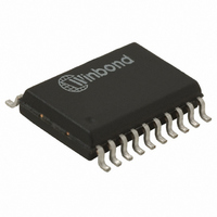
W6810ISG Nuvoton Technology Corporation of America, W6810ISG Datasheet - Page 12

W6810ISG
Manufacturer Part Number
W6810ISG
Description
IC VOICEBAND CODEC 5V 1CH 20SOP
Manufacturer
Nuvoton Technology Corporation of America
Type
PCMr
Specifications of W6810ISG
Data Interface
PCM Audio Interface
Resolution (bits)
8 b
Number Of Adcs / Dacs
1 / 1
Sigma Delta
No
Voltage - Supply, Analog
4.5 V ~ 5.5 V
Voltage - Supply, Digital
4.5 V ~ 5.5 V
Operating Temperature
-40°C ~ 85°C
Mounting Type
Surface Mount
Package / Case
20-SOP
Lead Free Status / RoHS Status
Lead free / RoHS Compliant
For Use With
W6810ES - EVALUATION SYSTEM FOR W6810W6810DK - KIT DEV/EVAL FOR W6810
Lead Free Status / RoHS Status
Compliant, Lead free / RoHS Compliant
Available stocks
Company
Part Number
Manufacturer
Quantity
Price
Part Number:
W6810ISG
Manufacturer:
NUVOTON
Quantity:
20 000
word is being transmitted. The transmit data pin PCMT will become high impedance when the Frame
Sync signal FST becomes LOW while the data is transmitted or when half of the LSB is transmitted.
The internal decision logic will determine whether the next frame sync is a long or a short frame sync,
based on the previous frame sync pulse. To avoid bus collisions, the PCMT pin will be high
impedance for two frame sync cycles after every power down state. More detailed timing information
can be found in the interface timing section.
The W6810 operates in the Short Frame Sync Mode when the Frame Sync signal at pin FST is HIGH
for one and only one falling edge of the bit-clock at the BCLKT pin. On the following rising edge of the
bit-clock, the W6810 starts clocking out the data on the PCMT pin, which will also change from high to
low impedance state. The data transmit pin PCMT will go back to the high impedance state halfway
the LSB. The Short Frame Sync operation of the W6810 is based on an 8-bit data word. When
receiving data on the PCMR pin, the data is clocked in on the first falling edge after the falling edge
that coincides with the Frame Sync signal. The internal decision logic will determine whether the next
frame sync is a long or a short frame sync, based on the previous frame sync pulse. To avoid bus
collisions, the PCMT pin will be high impedance for two frame sync cycles after every power down
state. More detailed timing information can be found in the interface timing section.
The GCI interface mode is selected when the BCLKR pin is connected to V
sync cycles. It can be used as a 2B+D timing interface in an ISDN application. The GCI interface
consists of 4 pins : FSC (FST), DCL (BCLKT), Dout (PCMT) & Din (PCMR). The FSR pin selects
channel B1 or B2 for transmit and receive. Data transitions occur on the positive edges of the data
clock DCL. The Frame Sync positive edge is aligned with the positive edge of the data clock DCLK.
The data rate is running half the speed of the bit-clock. The channels B1 and B2 are transmitted
consecutively. Therefore, channel B1 is transmitted on the first 16 clock cycles of DCL and B2 is
transmitted on the second 16 clock cycles of DCL. For more timing information, see the timing section,
figs. 8.3 and 8.4.
The IDL interface mode is selected when the BCLKR pin is connected to V
sync cycles. It can be used as a 2B+D timing interface in an ISDN application. The IDL interface
consists of 4 pins : IDL SYNC (FST), IDL CLK (BCLKT), IDL TX (PCMT) & IDL RX (PCMR). The FSR
pin selects channel B1 or B2 for transmit and receive. The data for channel B1 is transmitted on the
first positive edge of the IDL CLK after the IDL SYNC pulse. The IDL SYNC pulse is one IDL CLK
cycle long. The data for channel B2 is transmitted on the eleventh positive edge of the IDL CLK after
the IDL SYNC pulse. The data for channel B1 is received on the first negative edge of the IDL CLK
after the IDL SYNC pulse. The data for channel B2 is received on the eleventh negative edge of the
IDL CLK after the IDL SYNC pulse. The transmit signal pin IDL TX becomes high impedance when
not used for data transmission and also in the time slot of the unused channel. For more timing
information, see the timing section.
7.4.2. Short Frame Sync
7.4.3. General Circuit Interface (GCI)
7.4.4. Interchip Digital Link (IDL)
- 12 -
Publication Release Date: January 2009
DD
SS
for two or more frame
for two or more frame
W6810
Revision A14


