TP3054N/NOPB National Semiconductor, TP3054N/NOPB Datasheet - Page 2
TP3054N/NOPB
Manufacturer Part Number
TP3054N/NOPB
Description
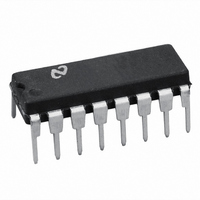
IC FILTER ENHANCE INTERFAC 16DIP
Manufacturer
National Semiconductor
Series
COMBO®r
Type
PCM Codec/Filterr
Datasheet
1.TP3054WMXNOPB.pdf
(16 pages)
Specifications of TP3054N/NOPB
Data Interface
Serial
Number Of Adcs / Dacs
1 / 1
Sigma Delta
No
Voltage - Supply, Analog
±5V
Voltage - Supply, Digital
±5V
Operating Temperature
-25°C ~ 125°C
Mounting Type
Through Hole
Package / Case
16-DIP (0.300", 7.62mm)
Lead Free Status / RoHS Status
Lead free / RoHS Compliant
Other names
*TP3054N
*TP3054N/NOPB
TP3054N
*TP3054N/NOPB
TP3054N


Block Diagram
Pin Description
V
GNDA
VF
V
FS
D
BCLK
MCLK
BB
CC
R
R
R
O
Symbol
R
R
CLKSEL The bit clock which shifts data into D
PDN
Negative power supply pin
V
Analog ground All signals are referenced
to this pin
Analog output of the receive power ampli-
fier
Positive power supply pin
V
Receive frame sync pulse which enables
BCLK
an 8 kHz pulse train See Figures 2 and 3
for timing details
Receive data input PCM data is shifted
into D
ter the FS
64 kHz to 2 048 MHz Alternatively may
be a logic input which selects either
1 536 MHz 1 544 MHz or 2 048 MHz for
master clock in synchronous mode and
BCLK
ceive directions (see Table I)
Receive
1 536 MHz 1 544 MHz or 2 048 MHz
May be asynchronous with MCLK
BB
CC
e b
e a
R
X
R
to shift PCM data into D
is used for both transmit and re-
following the FS
5V
5V
R
master
leading edge May vary from
g
g
5%
5%
Function
clock
R
leading edge
Must
R
FS
X
R
R
but
af-
be
is
FIGURE 1
2
MCLK
FS
BCLK
D
TS
GS
VF
VF
Symbol
X
X
X
X
X
X
I
I
b
a
X
X
should be synchronous with MCLK
formance When MCLK
ously low MCLK
ing When MCLK
high the device is powered down
Transmit master clock Must be 1 536 MHz
1 544 MHz or 2 048 MHz May be asynchronous
with MCLK
synchronous operation
Transmit frame sync pulse input which enables
BCLK
an 8 kHz pulse train see Figures 2 and 3 for
timing details
The bit clock which shifts out the PCM data on
D
must be synchronous with MCLK
The TRI-STATE PCM data output which is en-
abled by FS
Open drain output which pulses low during the
encoder time slot
Analog output of the transmit input amplifier
Used to externally set gain
Inverting input of the transmit input amplifier
Non-inverting input of the transmit input amplifi-
er
X
May vary from 64 kHz to 2 048 MHz but
X
to shift out the PCM data on D
R
X
Best performance is realized from
X
R
is selected for all internal tim-
Function
is connected continuously
R
is connected continu-
X
X
for best per-
TL H 5510 – 2
X
FS
X
is
Related parts for TP3054N/NOPB
Image
Part Number
Description
Manufacturer
Datasheet
Request
R

Part Number:
Description:
Serial Interface CODEC IC
Manufacturer:
National Semiconductor
Datasheet:

Part Number:
Description:
IC ENHANCED INTERFACE SER 16-DIP
Manufacturer:
National Semiconductor
Datasheet:
Part Number:
Description:
National Semiconductor [8-Bit D/A Converter]
Manufacturer:
National Semiconductor
Datasheet:
Part Number:
Description:
National Semiconductor [Media Coprocessor]
Manufacturer:
National Semiconductor
Datasheet:
Part Number:
Description:
Digitally Controlled Tone and Volume Circuit with Stereo Audio Power Amplifier, Microphone Preamp Stage and National 3D Sound
Manufacturer:
National Semiconductor
Datasheet:
Part Number:
Description:
Digitally Controlled Tone and Volume Circuit with Stereo Audio Power Amplifier, Microphone Preamp Stage and National 3D Sound
Manufacturer:
National Semiconductor
Datasheet:
Part Number:
Description:
AC97 Rev 2 Codec with Sample Rate Conversion and National 3D Sound
Manufacturer:
National Semiconductor
Part Number:
Description:
Manufacturer:
National Semiconductor
Datasheet:
Part Number:
Description:
Manufacturer:
National Semiconductor
Datasheet:
Part Number:
Description:
General Purpose, Low Voltage, Low Power, Rail-to-Rail Output Operational Amplifiers
Manufacturer:
National Semiconductor
Datasheet:
Part Number:
Description:
8-bit 20 MSPS flash A/D converter.
Manufacturer:
National Semiconductor
Datasheet:
Part Number:
Description:
Low Noise Quad Operational Amplifier
Manufacturer:
National Semiconductor
Datasheet:
Part Number:
Description:
Quad Differential Line Receivers
Manufacturer:
National Semiconductor
Datasheet:
Part Number:
Description:
Quad High Speed Trapezoidal? Bus Transceiver
Manufacturer:
National Semiconductor
Datasheet: