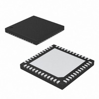
MAX9853ETM+T Maxim Integrated Products, MAX9853ETM+T Datasheet - Page 68

MAX9853ETM+T
Manufacturer Part Number
MAX9853ETM+T
Description
IC CODEC AUDIO STEREO 48TQFN
Manufacturer
Maxim Integrated Products
Type
Stereo Audior
Datasheet
1.MAX9851ETM.pdf
(71 pages)
Specifications of MAX9853ETM+T
Data Interface
Serial
Resolution (bits)
18 b
Number Of Adcs / Dacs
2 / 2
Sigma Delta
Yes
S/n Ratio, Adcs / Dacs (db) Typ
81.5 / 88
Dynamic Range, Adcs / Dacs (db) Typ
82 / 87.5
Voltage - Supply, Analog
2.6 V ~ 3.3 V
Voltage - Supply, Digital
1.7 V ~ 3.3 V
Operating Temperature
-40°C ~ 85°C
Mounting Type
Surface Mount
Package / Case
48-TQFN Exposed Pad
Lead Free Status / RoHS Status
Lead free / RoHS Compliant
Stereo Audio CODECs with Microphone, DirectDrive
Headphones, Speaker Amplifiers, or Line Outputs
Proper layout and grounding are essential for optimum
performance. Use large traces for the power-supply
inputs and amplifier outputs to minimize losses due to
parasitic trace resistance. Large traces also aid in mov-
ing heat away from the package. Proper grounding
improves audio performance, minimizes crosstalk
between channels, and prevents any switching noise
from coupling into the audio signal. Connect AGND,
DGND, CPGND, and PGND (MAX9851 only) together
at a single point on the PC board using the star ground-
ing technique. Route DGND, CPGND, and all traces
that carry switching transients or digital signals sepa-
rately from AGND and analog audio signal paths.
Ground all components associated with the charge
pump to CPGND (CPV
bypassing). Connect all digital I/O termination to DGND
including DV
PV
to PGND. Bypass V
analog ground (AGND).
Table 46. I
68
0x12
0x13
0x14
0x15
0x16
0x17
0x18
0x19
0x1A
0x1B
0x05
DD
______________________________________________________________________________________
REGISTER (hex)
pins on the MAX9851 (Class D power supplies)
DD
2
PC Board Layout and Bypassing
C Register Settings for Stereo Audio Record Mode (continued)
and DV
REF
, MBIAS, INTMICBIAS to a quiet
DDS2
SS
0x06
0x00
0x00
0x00
0x00
0x00
0x00
0x00
0xD5
0x33
0x89
bypassing and CPV
bypassing. Bypass both
VALUE (hex)
Select the external microphone interface and enable the external
microphone bias circuitry using 2.2kΩ bias resistors.
No configuration necessary
No configuration necessary
No configuration necessary
No configuration necessary
No configuration necessary
No configuration necessary
No configuration necessary
Enable the MAX9851/MAX9853 and configure the charge-pump circuitry
to run from MCLK (charge pump required to set AOK = 1 and allow
digital circuitry to operate)
Enable the ADC and microphone interface
Enable secondary digital audio interface and configure for output
operation at 48kHz stereo audio mode
DD
Connect PV
place the charge-pump capacitors as close to SV
possible. Ensure C2 is connected to CPGND and
bypass CPV
capacitors as close to the device as possible.
The MAX9851/MAX9853 thin QFN package features an
exposed thermal pad on its underside. This pad lowers
the package’s thermal resistance by providing a direct-
heat conduction path from the die to the PC board. If
possible, connect the exposed thermal pad to an elec-
trically isolated, large pad of copper. If it cannot be left
floating, connect it to AGND.
An evaluation kit (EV kit) is available to provide exam-
ple layouts for the MAX9851 and MAX9853. The EV kit
allows quick setup of the MAX9851/MAX9853 and
includes easy-to-use software allowing all internal reg-
isters to be controlled.
SS
DD
and SV
with 1µF to CPGND. Place the bypass
DESCRIPTION
SS
together at the device and
SS
as


