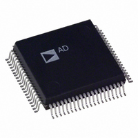
AD1843JS Analog Devices Inc, AD1843JS Datasheet - Page 21

AD1843JS
Manufacturer Part Number
AD1843JS
Description
IC CODEC STEREO 5V 16BIT 80PQFP
Manufacturer
Analog Devices Inc
Type
Stereo Audior
Datasheet
1.AD1843JS.pdf
(64 pages)
Specifications of AD1843JS
Rohs Status
RoHS non-compliant
Data Interface
Serial
Resolution (bits)
16 b
Number Of Adcs / Dacs
1 / 2
Sigma Delta
Yes
S/n Ratio, Adcs / Dacs (db) Typ
92 / 86
Dynamic Range, Adcs / Dacs (db) Typ
85 / 80
Voltage - Supply, Analog
4.75 V ~ 5.25 V
Voltage - Supply, Digital
2.85 V ~ 5.25 V
Operating Temperature
0°C ~ 70°C
Mounting Type
Surface Mount
Package / Case
80-MQFP, 80-PQFP
Available stocks
Company
Part Number
Manufacturer
Quantity
Price
Part Number:
AD1843JS
Manufacturer:
ADI/亚德诺
Quantity:
20 000
REV. 0
interval to update the DAC Not Full status bits. Therefore
driver software does not have to make provision for frame-to-
frame delays between control and status information; the infor-
mation in each frame is always up to date.
The AD1843 supports locking to an external clock which may
result in a sample rate that is marginally higher than the nominal
audio standard maximum sample rate of 48 kHz. This is neces-
sary since two crystal-based clock sources are never perfectly
matched to one another. One is always at a slightly higher fre-
quency. The AD1843 conversion channels have been designed
to support sample rates that are up to 2.1% higher than 48 kHz
(i.e., 49 kHz), referenced to the AD1843’s clock input on
XTALI, when all conversion channels are simultaneously run-
ning. Even higher rates can be supported when all channels are
not running simultaneously. See the “Conversion Rates” sec-
tion above for additional details. The serial interface must also
allow for this higher sample rate with a frame sync (SDFS) rate
that is at least as high as the sample rate in 16 slot per frame
DAC1, DAC2
DAC1, DAC2
STEREO
STEREO
16-BIT
16-BIT
MONO
MONO
8-BIT
8-BIT
SCLK
SDFS
SDO
SDO
SDO
SDO
SDI
SDI
SDI
SDI
THE DIAGRAM ABOVE IS INTENDED TO BE ILLUSTRATIVE OF THE MORE COMMONLY USED CONFIGURATIONS. ADC LEFT, ADC RIGHT, DAC1
AND DAC2 CAN BE INDIVIDUALLY ASSIGNED TO 8-BIT OR 16-BIT SAMPLE WIDTH, AND DAC1 AND DAC2 CAN BE INDIVIDUALLY ASSIGNED
TO STEREO OR MONO MODE. EACH AD1843 CONSUMES 6 TMD SLOTS (REQUIRING 96 SCLK PERIODS), LEAVING 10 TDM SLOTS
UNUSED IN A 16 SLOT FRAME.
NOTE THAT BECAUSE THE SERIAL INTERFACE AND THE ADC AND DACS ARE IN GENERAL ASYNCHRONOUS, NOT EVERY CAPTURE OR
PLAYBACK TIME SLOT WILL CONTAIN VALID DATA. THE HOST PROCESSOR MUST POLL THE STATUS WORD TO DETERMINE WHETHER
THE ADC DATA IS VALID AND WHETHER THE DAC IS REQUESTING ADDITIONAL SAMPLES.
IGNORED
3-STATED
IGNORED
3-STATED
IGNORED
3-STATED
IGNORED
3-STATED
CONTROL WORD
CONTROL WORD
CONTROL WORD
CONTROL WORD
STATUS WORD
STATUS WORD
STATUS WORD
STATUS WORD
SLOT 0
16 BITS
TIME
Figure 11. AD1843 Slot Assignments
REGISTER DATA
REGISTER DATA
REGISTER DATA
REGISTER DATA
REGISTER DATA
REGISTER DATA
REGISTER DATA
REGISTER DATA
SLOT 1
TIME
–21–
DAC1L
ADCL
DAC1
ADCL
DAC1 LEFT
ADC LEFT
ADC LEFT
SLOT 2
DAC1
mode, or half as high as the sample rate in 32 slot per frame
mode. When the AD1843 is bus master, the SCLK frequency
is either 12.288 MHz or 16.384 MHz, which allows for up to
48 kHz or 64 kHz sampling rates, respectively.
The AD1843 Control Registers are read and written by trans-
mitting a read/write request bit along with the Control Register
address in the slot 0 Control Word. When a read is requested,
the contents of the Control Register addressed is transmitted
out during slot 1 of the following frame. When a write is re-
quested, data to be written must be transmitted to the AD1843
in slot 1, and the former contents of the control register are
transmitted out during slot 1 of the following frame. Unless oth-
erwise noted, Control Register writes do not take effect until the
current round of six communication TDM time slots concludes.
Equivalently, unless otherwise noted, Control Register writes do
not take effect until the subsequent falling edge of the TSO signal.
The following sections describe the bit assignments for all time
slots.
TIME
DON'T
DON'T
CARE
CARE
0s
0s
DAC1R
ADCR
ADCR
DON'T CARE
DON'T CARE
DAC1 RIGHT
ADC RIGHT
ADC RIGHT
SLOT 3
TIME
DON'T
CARE
0s
0s
DAC2L
DAC2
DAC2 LEFT
SLOT 4
DAC2
TIME
0s
0s
0s
0s
DON'T
CARE
DON'T
CARE
DAC2R
DON'T CARE
DON'T CARE
DAC2 RIGHT
SLOT 5
TIME
0s
0s
0s
0s
DON'T
CARE
AD1843
IGNORED
3-STATED
IGNORED
3-STATED
IGNORED
3-STATED
IGNORED
3-STATED


