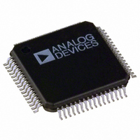
ADV7202KST Analog Devices Inc, ADV7202KST Datasheet - Page 12

ADV7202KST
Manufacturer Part Number
ADV7202KST
Description
IC CODEC VIDEO 10BIT 64LQFP
Manufacturer
Analog Devices Inc
Type
Video Codecr
Datasheet
1.ADV7202KSTZ.pdf
(28 pages)
Specifications of ADV7202KST
Rohs Status
RoHS non-compliant
Data Interface
Serial
Resolution (bits)
12, 10 b
Number Of Adcs / Dacs
1 / 4
Sigma Delta
No
Voltage - Supply, Analog
4.75 V ~ 5.25 V
Voltage - Supply, Digital
4.75 V ~ 5.25 V
Operating Temperature
0°C ~ 70°C
Mounting Type
Surface Mount
Package / Case
64-LQFP
Lead Free Status / Rohs Status
Not Compliant
Available stocks
Company
Part Number
Manufacturer
Quantity
Price
Company:
Part Number:
ADV7202KST
Manufacturer:
CSR
Quantity:
1 000
Company:
Part Number:
ADV7202KSTZ
Manufacturer:
Analog Devices Inc
Quantity:
10 000
ADV7202
MPU PORT DESCRIPTION
The ADV7202 supports a 2-wire serial (I
microprocessor bus driving multiple peripherals. Two inputs,
serial data (SDA) and serial clock (SCL), carry information
between any device connected to the bus. Each slave device is
recognized by a unique address. The ADV7202 has four pos-
sible slave addresses for both read and write operations. These
are unique addresses for each device and are illustrated in
Figure 4. The LSB sets either a read or write operation. Logic
Level “1” corresponds to a read operation, while Logic Level
“0” corresponds to a write operation. A1 is set by setting the
ALSB pin of the ADV7202 to Logic Level “0” or Logic Level
“1.” When ALSB is set to “0,” there is greater input bandwidth
on the I
bus. When ALSB is set to “1,” there is reduced input band-
width on the I
50 ns will not pass into the I
recommended for noisy systems.
To control the various devices on the bus, the following proto-
col must be followed. First, the master initiates a data transfer by
establishing a Start condition, defined by a high-to-low transition
on SDA while SCL remains high. This indicates that an address/
data stream will follow. All peripherals respond to the Start
condition and shift the next eight bits (7-bit address + R/W bit).
The bits are transferred from MSB down to LSB. The periph-
eral that recognizes the transmitted address responds by pulling
the data line low during the ninth clock pulse. This is known as
an Acknowledge Bit. All other devices withdraw from the bus at
this point and maintain an idle condition. The idle condition
is where the device monitors the SDA and SCL lines waiting for
the Start condition and the correct transmitted address. The R/W
bit determines the direction of the data.
0
2
C lines, which allows high speed data transfers on this
0
2
C lines, which means that pulses of less than
Figure 4. Slave Address
1
SYNC_OUT
DOUT [9:0]
0
2
C internal controller. This mode is
XTAL0
1
Figure 3. SYNC_OUT Output Timing, YCrCb Input
CR
2
1
C-compatible)
0
1
ADDRESS
CONTROL
SET UP BY
READ/WRITE
ALSB
CONTROL
A1
DISABLED
ENABLED
Y
X
CB
–12–
A Logic “0” on the LSB of the first byte means that the master
will write information to the peripheral. A Logic “1” on the LSB
of the first byte means that the master will read information
from the peripheral.
The ADV7202A acts as a standard slave device on the bus. The
data on the SDA pin is eight bits long, supporting the 7-bit
addresses plus the R/W bit. It interprets the first byte as the
device address and the second byte as the starting subaddress.
The subaddresses auto-increment, allowing data to be written to
or read from the starting subaddress. A data transfer is always
terminated by a Stop condition. The user can access any unique
subaddress register one-by-one, without updating all the registers.
Stop and Start conditions can be detected at any stage during
the data transfer. If these conditions are asserted out of sequence
with normal read and write operations, they cause an immediate
jump to the idle condition. During a given SCL high period, the
user should only issue one Start condition, one Stop condition,
or a single Stop condition followed by a single Start condition. If
an invalid subaddress is issued by the user, the ADV7202 will
not issue an acknowledge and will return to the idle condition. If
in auto-increment mode, the user exceeds the highest subaddress,
the following action will be taken:
1. In read mode, the highest subaddress register contents
2. In write mode, the data for the invalid byte will not be
Figure 5 illustrates an example of data transfer for a read
sequence and the Start and Stop conditions.
SCLOCK
SDATA
Y
will continue to be output until the master device issues a
no-acknowledge. This indicates the end of a read. A
no-acknowledge condition is where the SDA line is not
pulled low on the ninth pulse.
loaded into any subaddress register, a no-acknowledge will
be issued by the ADV7202, and the part will return to the
idle condition.
START ADDR R/W ACK SUBADDRESS ACK
S
CR
1–7
Figure 5. Bus Data Transfer
8
Y
9
1–7
CB
8
9
DATA
1–7
8
ACK
9
REV. 0
STOP
P


