LAN83C185-JT SMSC, LAN83C185-JT Datasheet - Page 13
LAN83C185-JT
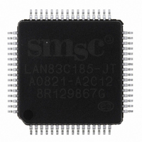
Manufacturer Part Number
LAN83C185-JT
Description
IC PHY 10/100 3.3V LP 64-TQFP
Manufacturer
SMSC
Datasheet
1.LAN83C185-JT.pdf
(60 pages)
Specifications of LAN83C185-JT
Controller Type
Ethernet Controller
Interface
MII
Voltage - Supply
3 V ~ 3.6 V
Current - Supply
40mA
Operating Temperature
0°C ~ 70°C
Mounting Type
Surface Mount
Package / Case
64-TQFP, 64-VQFP
Supply Voltage Range
2.97V To 3.63V
Digital Ic Case Style
TQFP
No. Of Pins
64
Operating Temperature Range
0°C To +70°C
Data Rate Max
100Mbps
Supply Voltage Max
3.6V
Rohs Compliant
Yes
Lead Free Status / RoHS Status
Lead free / RoHS Compliant
Other names
638-1009
Available stocks
Company
Part Number
Manufacturer
Quantity
Price
Company:

Part Number:
LAN83C185-JT
Manufacturer:
Standard
Quantity:
2 077
Company:
Part Number:
LAN83C185-JT
Manufacturer:
ALTERA
Quantity:
513
Company:
Part Number:
LAN83C185-JT
Manufacturer:
Microchip Technology
Quantity:
10 000


High Performance Single Chip Low Power 10/100 Ethernet Physical Layer Transceiver (PHY)
Datasheet
SMSC LAN83C185
PIN NO.
PIN NO.
20
19
17
16
10
12
46
25
23
22
64
11
2
6
5
4
9
3
2
PHYAD4
PHYAD3
PHYAD2
PHYAD1
PHYAD0
MODE2
MODE1
MODE0
TEST1
TEST0
REG_EN
nINT
nRST
CLKIN/XTAL1
XTAL2
CLK_FREQ
NC1
GPO2
GPO1
SIGNAL NAME
SIGNAL NAME
Table 3.4 Configuration Inputs
Table 3.5 General Signals
I
I
I
I
I
I
I
I
I
I
I
OD
I
I
O
I
O
O
TYPE
TYPE
DATASHEET
PHY Address Bit 4: set the default address of the PHY.
PHY Address Bit 3: set the default address of the PHY.
PHY Address Bit 2: set the default address of the PHY.
PHY Address Bit 1: set the default address of the PHY.
PHY Address Bit 0: set the default address of the PHY.
PHY Operating Mode Bit 2: set the default MODE of the
PHY. See
page 46
PHY Operating Mode Bit 1: set the default MODE of the
PHY. See
page 46
PHY Operating Mode Bit 0: set the default MODE of the
PHY. See
page 46
Test Mode Select 1: Must be left floating.
Test Mode Select 0: Must be left floating.
Internal +1.8V Regulator Enable:
+3.3V – Enables internal regulator.
0V – Disables internal regulator.
13
LAN Interrupt – Active Low output.
External Reset – input of the system reset. This signal is
active LOW.
Clock Input – 25 MHz external clock or crystal input.
Clock Output – 25 MHz crystal output.
Clock Frequency – define the frequency of the input
clock CLKIN
0 – Clock frequency is 25 MHz.
1 – Reserved.
This input needs to be held low continuously, during and
after reset. This pin should be pulled-down to VSS via a
pull-down resistor.
No Connect
General Purpose Output 2 – General Purpose Output
signal Driven by bits in registers 27 and 31.
General Purpose Output 1 – General Purpose Output
signal Driven by bits in registers 27 and 31.
(Muxed with PHYAD4 signal)
for the MODE options.
for the MODE options.
for the MODE options.
Section 5.4.9.2, "Mode Bus – MODE[2:0]," on
Section 5.4.9.2, "Mode Bus – MODE[2:0]," on
Section 5.4.9.2, "Mode Bus – MODE[2:0]," on
DESCRIPTION
DESCRIPTION
Revision 0.8 (06-12-08)
Related parts for LAN83C185-JT
Image
Part Number
Description
Manufacturer
Datasheet
Request
R


Part Number:
Description:
FAST ETHERNET PHYSICAL LAYER DEVICE
Manufacturer:
SMSC Corporation
Datasheet:
Part Number:
Description:
357-036-542-201 CARDEDGE 36POS DL .156 BLK LOPRO
Manufacturer:
SMSC Corporation
Datasheet:
Part Number:
Description:
357-036-542-201 CARDEDGE 36POS DL .156 BLK LOPRO
Manufacturer:
SMSC Corporation
Datasheet:
Part Number:
Description:
357-036-542-201 CARDEDGE 36POS DL .156 BLK LOPRO
Manufacturer:
SMSC Corporation
Datasheet:
Part Number:
Description:
4-PORT USB2.0 HUB CONTROLLER
Manufacturer:
SMSC Corporation
Datasheet:
Part Number:
Description:
Manufacturer:
SMSC Corporation
Datasheet:
Part Number:
Description:
Manufacturer:
SMSC Corporation
Datasheet:
Part Number:
Description:
FDC37C672ENHANCED SUPER I/O CONTROLLER WITH FAST IR
Manufacturer:
SMSC Corporation
Datasheet:
Part Number:
Description:
COM90C66LJPARCNET Controller/Transceiver with AT Interface and On-Chip RAM
Manufacturer:
SMSC Corporation
Datasheet:
Part Number:
Description:
Manufacturer:
SMSC Corporation
Datasheet:
Part Number:
Description:
Manufacturer:
SMSC Corporation
Datasheet:
Part Number:
Description:
Manufacturer:
SMSC Corporation
Datasheet:
Part Number:
Description:
Manufacturer:
SMSC Corporation
Datasheet: