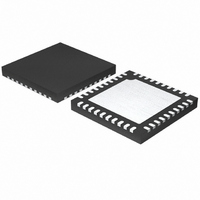
SI3453A-B01-GM Silicon Laboratories Inc, SI3453A-B01-GM Datasheet - Page 25

SI3453A-B01-GM
Manufacturer Part Number
SI3453A-B01-GM
Description
IC POE CONTROLLER MIDSPAN 40QFN
Manufacturer
Silicon Laboratories Inc
Specifications of SI3453A-B01-GM
Package / Case
40-QFN
Controller Type
Power over Ethernet Controller (POE)
Interface
I²C
Voltage - Supply
3 V ~ 3.6 V
Current - Supply
14mA
Operating Temperature
-40°C ~ 85°C
Mounting Type
Surface Mount
Maximum Power Dissipation
1.2 W
Minimum Operating Temperature
- 40 C
Mounting Style
SMD/SMT
Product
Ethernet Controllers
Standard Supported
IEEE 802.3at, IEEE 802.3af
Supply Voltage (max)
3.6 V
Supply Voltage (min)
3 V
Supply Current (max)
14 mA
Maximum Operating Temperature
+ 85 C
Lead Free Status / RoHS Status
Lead free / RoHS Compliant
Lead Free Status / RoHS Status
Lead free / RoHS Compliant, Lead free / RoHS Compliant
Other names
336-1838-5
7. PCB Layout Guidelines
Due to the high current of up to 800 mA per port, the following board layout guidelines apply. In addition, contact
Silicon Laboratories. for access to complete PSE reference design databases including recommended layouts.
The VEE1, VEE2, VEE3 and VEE4 pins can carry up to 800 mA and are connected to a V
a 24 port PCB layout could thus carry as much as 20 A current. With 2 oz. copper on an outer layer, a bus of 0.4
inches is needed. For an inner layer, this increases to 1 inch wide bus. Use of large or multiple vias is required for
properly supporting the 800 mA per channel operating current. The VEE pin does not carry high current and can be
connected directly to the bus as well. The best practice is to devote an entire inner layer for V
Similarly, GND1/2 and GND3/4 pins can carry up to 1.6 A per pin and the GND return bus should be at least as
wide as the V
ground power plane does not generally have a high frequency content (other than external faults) so it is generally
acceptable to use the ground power plane as a ground signal plane and tie AGND and GND12, GND34 to this
plane as well.
The VOUTn pins carry up to 800 mA dc and up to 5 A in faults, so a 20 mil trace with wide or multiple vias are also
recommended. The VDETn pins also carry fault current so this pin connection to VOUTn needs to use 20 mil
traces and wide or multiple vias where needed.
The VDD currents are not large so it is acceptable to route the VDD nodes on one of the outer layers.
If care is taken to avoid disruption of the high current paths, VDD can be globally routed on one of the power planes
and then locally routed on an inner or outer layer.
To avoid coupling between surge events and logic signals, it is recommended that VOUTn traces be routed on the
opposite side as the I
The thermal pad of the Si3452/3 is connected to VEE. At full IEEE 802.3at current of 600 mA on each port the
dissipation of the Si3452/3 is up to 1.2 W; so, multiple vias are required to conduct the heat from the thermal pad to
the VEE plane. As many as 36 small vias provide the best thermal conduction.
EE
bus as above. The best practice is to devote an entire inner layer for ground power routing. The
2
C interface pins.
Rev. 0.42
EE
bus. The V
EE
Si3452/3
power routing.
EE
bus for
25


