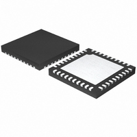
SI3453-B01-GM Silicon Laboratories Inc, SI3453-B01-GM Datasheet - Page 31

SI3453-B01-GM
Manufacturer Part Number
SI3453-B01-GM
Description
IC POE CONTROLLER MIDSPAN 40QFN
Manufacturer
Silicon Laboratories Inc
Specifications of SI3453-B01-GM
Package / Case
40-QFN
Controller Type
Power over Ethernet Controller (POE)
Interface
I²C
Voltage - Supply
3 V ~ 3.6 V
Current - Supply
14mA
Operating Temperature
-40°C ~ 85°C
Mounting Type
Surface Mount
Maximum Power Dissipation
1.2 W
Minimum Operating Temperature
- 40 C
Mounting Style
SMD/SMT
Product
Ethernet Controllers
Standard Supported
IEEE 802.3at, IEEE 802.3af
Supply Voltage (max)
3.6 V
Supply Voltage (min)
3 V
Supply Current (max)
14 mA
Maximum Operating Temperature
+ 85 C
Lead Free Status / RoHS Status
Lead free / RoHS Compliant
Lead Free Status / RoHS Status
Lead free / RoHS Compliant, Lead free / RoHS Compliant
Other names
336-1837-5
Notes:
General
Solder Mask Design
Stencil Design
Card Assembly
1. All dimensions shown are in millimeters (mm) unless otherwise noted.
2. Dimensioning and Tolerancing is per the ANSI Y14.5M-1994 specification.
3. This Land Pattern Design is based on IPC-SM-782 guidelines.
4. All dimensions shown are at Maximum Material Condition (MMC). Least Material
5. All metal pads are to be non-solder mask defined (NSMD). Clearance between the
6. A stainless steel, laser-cut and electro-polished stencil with trapezoidal walls should
7. The stencil thickness should be 0.125 mm (5 mils).
8. The ratio of stencil aperture to land pad size should be 1:1 for the perimeter pads.
9. A 4x4 array of 0.80 mm square openings on 1.05 mm pitch should be used for the
10. A No-Clean, Type-3 solder paste is recommended.
11. The recommended card reflow profile is per the JEDEC/IPC J-STD-020C
Condition (LMC) is calculated based on a Fabrication Allowance of 0.05 mm.
solder mask and the metal pad is to be 60 µm minimum, all the way around the pad.
be used to assure good solder paste release.
center ground pad.
specification for Small Body Components.
Dimension
Table 26. PCB Land Pattern Dimensions (Continued)
ZD
Rev. 0.42
Min
—
Max
6.31
Si3452/3
31


