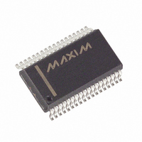
MAX5945CAX+ Maxim Integrated Products, MAX5945CAX+ Datasheet - Page 20

MAX5945CAX+
Manufacturer Part Number
MAX5945CAX+
Description
IC NETWORK PWR CTRL 36-SSOP
Manufacturer
Maxim Integrated Products
Datasheet
1.MAX5945CAX.pdf
(44 pages)
Specifications of MAX5945CAX+
Controller Type
Network Power Controller
Interface
I²C
Voltage - Supply
3.3V
Current - Supply
4.2mA
Operating Temperature
0°C ~ 70°C
Mounting Type
Surface Mount
Package / Case
36-SSOP
Lead Free Status / RoHS Status
Lead free / RoHS Compliant
Each clock pulse transfers one data bit (Figure 8). The
data on SDA must remain stable while SCL is high.
The acknowledge bit is a clocked 9th bit (Figure 9),
which the recipient uses as a handshake receipt of each
byte of data. Thus each byte effectively transferred
requires 9 bits. The master generates the 9th clock
pulse, and the recipient pulls down SDA (or the SDAOUT
in the 3-wire interface) during the acknowledge clock
pulse, so the SDA line is stable low during the high peri-
od of the clock pulse. When the master transmits to the
MAX5945, the MAX5945 generates the acknowledge bit.
When the MAX5945 transmits to the master, the master
generates the acknowledge bit.
The MAX5945 has a 7-bit long slave address (Figure
10). The bit following the 7-bit slave address (bit eight)
is the R/W bit, which is low for a write command and
high for a read command.
010 always represent the first three bits (MSBs) of the
MAX5945 slave address. Slave address bits A3, A2,
A1, and A0 represent the states of the MAX5945’s A3,
A2, A1, and A0 inputs, allowing up to sixteen MAX5945
devices to share the bus. The states of the A3, A2, A1,
Quad Network Power Controller
for Power-Over-LAN
Figure 9. Acknowledge
Figure 10. Slave Address
20
______________________________________________________________________________________
SDA
SCL
BY TRANSMITTER
MSB
0
BY RECEIVER
SDA
SDA
SCL
START CONDITION
1
S
0
Slave Address
1
Acknowledge
Bit Transfer
A3
2
A2
and A0 latch in upon the reset of the MAX5945 into reg-
ister R11h. The MAX5945 monitors the bus continuous-
ly, waiting for a START condition followed by the
MAX5945’s slave address. When the MAX5945 recog-
nizes its slave address, it acknowledges and is then
ready for continued communication.
The global address call is used in writing mode to write
the same register to multiple devices (address 0x60). In
read mode (address 0x61), the global address call is
used as the alert response address. When responding to
a global call, the MAX5945 puts out on the data line its
own address whenever its interrupt is active and so does
every other device connected to the SDAOUT line that
has an active interrupt. After every bit is transmitted, the
MAX5945 checks that the data line effectively corre-
sponds to the data it is delivering. If it is not, it then backs
off and frees the data line. This litigation protocol always
allows the part with the lowest address to complete the
transmission. The microcontroller can then respond to
the interrupt and take proper actions. The MAX5945
does not reset its own interrupt at the end of the alert
response protocol. The microcontroller has to do it by
clearing the event register through their CoR addresses
or activating the CLR_INT pushbutton.
Global Addressing and Alert Response Protocol
CLOCK PULSE FOR ACKNOWLEDGEMENT
A1
8
LSB
A0
R/W
9
ACK


