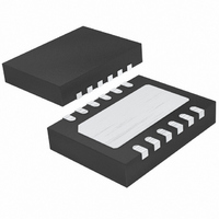
LTC4264IDE#PBF Linear Technology, LTC4264IDE#PBF Datasheet - Page 14

LTC4264IDE#PBF
Manufacturer Part Number
LTC4264IDE#PBF
Description
IC CNTRLR PD INTERFACE 12-DFN
Manufacturer
Linear Technology
Datasheet
1.LTC4264CDEPBF.pdf
(24 pages)
Specifications of LTC4264IDE#PBF
Controller Type
Power over Ethernet Controller (POE)
Interface
IEEE 802.3af
Current - Supply
3mA
Operating Temperature
-40°C ~ 85°C
Mounting Type
Surface Mount
Package / Case
12-DFN
Lead Free Status / RoHS Status
Lead free / RoHS Compliant
Voltage - Supply
-
Available stocks
Company
Part Number
Manufacturer
Quantity
Price
APPLICATIONS INFORMATION
LTC4264
The active high PWRGD pin features an internal, open-
collector output referenced to V
active high PWRGD pin pulls low until the load capacitor
is fully charged. At that point, PWRGD becomes high
impedance, indicating the converter may begin running.
The active high PWRGD pin can interface directly with the
“Run” pin of converter products. The PWRGD pin features
an internal 14V clamp to V
converter from excessive voltage. During a power supply
ramp down event, PWRGD becomes low impedance when
V
high impedance when the V
detection voltage range.
The active low PWRGD pin connects to an internal, open
drain MOSFET referenced to V
During inrush, PWRGD is high impedance. Once the load
capacitor is fully charged, PWRGD is pulled low and DC/DC
converter operation can begin. The active low PWRGD
pin can connect directly to the shutdown pin of converter
products. PWRGD is referenced to the V
active will be near the V
typically be referenced to V
ensure that the difference in potential of the PWRGD pin
does not cause a problem for the DC/DC converter. The
use of diode clamp D9 and R
alleviates any problems.
THERMAL PROTECTION
The LTC4264 includes thermal overload protection in
order to provide full device functionality in a miniature
package while maintaining safe operating temperatures.
At turn-on, before load capacitor C1 has charged up, the
instantaneous power dissipated by the LTC4264 can be
as high as 20W. As the load capacitor charges, the power
dissipation in the LTC4264 will decrease until it reaches
a steady-state value dependent on the DC load current.
The LTC4264 can also experience device heating after
turn-on if the PD experiences a fast input voltage rise. For
example, if the PD input voltage steps from –37V to –57V,
14
IN
drops below the UVLO turn-off threshold, then goes
IN
OUT
OUT
potential. The converter will
IN
S
which protects the DC/DC
voltages fall to within the
and care must be taken to
, as shown in Figure 11,
IN
OUT
which can sink 1mA.
. During inrush, the
IN
pin and when
the instantaneous power dissipated by the LTC4264 can
be as high as 16W.
The LTC4264 protects itself from damage by monitoring
die temperature. If the die exceeds the overtemperature
trip point, the power MOSFET and classifi cation transis-
tors are disabled until the part cools down. Once the die
cools below the overtemperature trip point, all functions
are enabled automatically.
During classifi cation, excessive heating of the LTC4264
can occur if the PSE violates the 75ms probing time limit.
In addition, the IEEE 802.3af specifi cation requires a PD
to withstand application of any voltage from 0V to 57V
indefi nitely. To protect the LTC4264 in these situations,
the thermal protection circuitry disables the classifi cation
circuit if the die temperature exceeds the overtemperature
trip point. When the die cools down, classifi cation current
is enabled.
Once the LTC4264 has charged up the load capacitor
and the PD is powered and running, there will be some
residual heating due to the DC load current of the PD
fl owing through the internal MOSFET. In some high cur-
rent applications, the LTC4264 power dissipation may be
signifi cant. The LTC4264 uses a thermally enhanced DFN12
package that includes an Exposed Pad which should be
soldered to an electrically isolated heat sink on the printed
circuit board.
MAXIMUM AMBIENT TEMPERATURE
The LTC4264 I
the normal operating current limit. With the normal cur-
rent limit disabled, it is possible to pass currents as high
as 1.4A through the LTC4264. In this mode, signifi cant
package heating may occur. Depending on the current,
voltage, ambient temperature, and waveform character-
istics, the LTC4264 may shut down. To avoid nuisance
trips of the thermal shutdown, it may be necessary to
limit the maximum ambient temperature. Limiting the die
temperature to 125°C will keep the LTC4264 from hitting
LIM_EN
pin allows the PD designer to disable
4264f


