USBN9603-28MX/NOPB National Semiconductor, USBN9603-28MX/NOPB Datasheet - Page 14
USBN9603-28MX/NOPB
Manufacturer Part Number
USBN9603-28MX/NOPB
Description
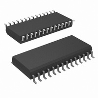
IC CTRLR FULL SPD FUNC 28-SOIC
Manufacturer
National Semiconductor
Datasheet
1.USBN9604-28MNOPB.pdf
(60 pages)
Specifications of USBN9603-28MX/NOPB
Controller Type
USB 2.0 Controller
Interface
Parallel/Serial
Voltage - Supply
3 V ~ 5.5 V
Current - Supply
30mA
Operating Temperature
0°C ~ 70°C
Mounting Type
Surface Mount
Package / Case
28-SOIC (7.5mm Width)
For Use With
USBN9604-HS-EB - KIT NODE CONTROLLER SAMPLE
Lead Free Status / RoHS Status
Lead free / RoHS Compliant
Other names
*USBN9603-28MX
*USBN9603-28MX/NOPB
USBN9603-28MX
*USBN9603-28MX/NOPB
USBN9603-28MX
Available stocks
Company
Part Number
Manufacturer
Quantity
Price
Company:

Part Number:
USBN9603-28MX/NOPB
Manufacturer:
NS
Quantity:
3 000
Part Number:
USBN9603-28MX/NOPB
Manufacturer:
NS/国半
Quantity:
20 000


www.national.com
3.0 Parallel Interface
3.1.1
The standard access sequence for non-multiplexed mode is to write the address to the ADDR register and then read or write
the data from/to the DATA_OUT/DATA_IN register. The DATA_OUT register is updated after writing to the ADDR register.
The ADDR register or the DATA_OUT/DATA_IN register is selected with the A0 input.
3.1.2
In burst mode, the ADDR register is written once with the desired memory address of any of the on-chip registers. Then
consecutive reads/writes are performed to the DATA_IN/DATA_OUT register without previously writing a new address. The
content of the DATA_OUT register for read operations is updated once after every read or write.
3.1.3
The following table gives an overview of the parallel interface registers in non-multiplexed mode.
The reserved bits return undefined data on read and should be written with 0.
Address Register (ADDR)
The ADDR register acts as a pointer to the internal memory. This register is write only and is cleared on reset.
Data Output Register (DATA_OUT)
The DATA_OUT register is updated with the contents of the memory register to which the ADDR register is pointing. Update
occurs under the following conditions:
1. After the ADDR register is written.
2. After a read from the DATA_OUT register.
3. After a write to the DATA_IN register.
This register is read only and holds undefined data after reset.
Data Input Register (DATA_IN)
The DATA_IN register holds the data written to the device address to which ADDR points. This register is write only and is
cleared on reset.
Standard Access Mode
Burst Mode
User Registers
A0
0
0
1
1
Access
Read
Write
Read
Write
(Continued)
bit 7
Reserved
bit 6
bit 5
14
bit 4
DATA_OUT
Reserved
DATA_IN
bit 3
ADDR5-0
bit 2
bit 1
bit 0
Related parts for USBN9603-28MX/NOPB
Image
Part Number
Description
Manufacturer
Datasheet
Request
R

Part Number:
Description:
IC CONTROLLER USB 28-SOIC
Manufacturer:
National Semiconductor
Datasheet:

Part Number:
Description:
USB Controller IC
Manufacturer:
National Semiconductor
Datasheet:

Part Number:
Description:
USBN9603 Universal Serial Bus Full Speed Function Controller with Enhanced DMA Support
Manufacturer:
National Semiconductor
Datasheet:
Part Number:
Description:
Universal Serial Bus Full Speed Node Controller with Enhanced DMA Support
Manufacturer:
National Semiconductor
Part Number:
Description:
USBN9603/USBN9604 Universal Serial Bus Full Speed Node Controller with Enhanced DMA Support
Manufacturer:
National Semiconductor
Datasheet:
Part Number:
Description:
National Semiconductor [8-Bit D/A Converter]
Manufacturer:
National Semiconductor
Datasheet:
Part Number:
Description:
National Semiconductor [Media Coprocessor]
Manufacturer:
National Semiconductor
Datasheet:
Part Number:
Description:
Digitally Controlled Tone and Volume Circuit with Stereo Audio Power Amplifier, Microphone Preamp Stage and National 3D Sound
Manufacturer:
National Semiconductor
Datasheet:
Part Number:
Description:
Digitally Controlled Tone and Volume Circuit with Stereo Audio Power Amplifier, Microphone Preamp Stage and National 3D Sound
Manufacturer:
National Semiconductor
Datasheet:
Part Number:
Description:
AC97 Rev 2 Codec with Sample Rate Conversion and National 3D Sound
Manufacturer:
National Semiconductor
Part Number:
Description:
Manufacturer:
National Semiconductor
Datasheet:
Part Number:
Description:
Manufacturer:
National Semiconductor
Datasheet:
Part Number:
Description:
General Purpose, Low Voltage, Low Power, Rail-to-Rail Output Operational Amplifiers
Manufacturer:
National Semiconductor
Datasheet: