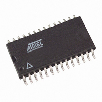
AT83C24B-TISUM Atmel, AT83C24B-TISUM Datasheet - Page 11

AT83C24B-TISUM
Manufacturer Part Number
AT83C24B-TISUM
Description
IC SMART CARD READER 5V 28SOIC
Manufacturer
Atmel
Datasheet
1.AT83C24-PRTIL.pdf
(42 pages)
Specifications of AT83C24B-TISUM
Controller Type
Smart Card Reader Interface
Interface
2-Wire
Voltage - Supply
3 V ~ 5.5 V
Operating Temperature
-40°C ~ 85°C
Mounting Type
Surface Mount
Package / Case
28-SOIC (7.5mm Width)
Lead Free Status / RoHS Status
Lead free / RoHS Compliant
Current - Supply
-
CIO, CC4, CC8 Controller
Clock Controller
4234G–SCR–01/07
The CIO, CC4, CC8 output pins are driven respectively by CARDIO, CARDC4, CARDC8 bits
values or by I/O, C4, C8 signal pins. This selection depends of the IODIS bit value. If IODIS is
reset, data are bidirectional between respectively I/O, C4, C8 pins and CIO, CC4, CC8 pins.
IO and CIO pins are linked together through the on chip level shifters if IODIS bit=0 in INTER-
FACE register. This is done automatically during an hardware activation.
Their iddle level are 1. With IO high, CIO is pulled up.
The same behavior is applicable on C4/ CC4 and C8/ CC8 pins.
The maximum frequency on those lines depends on CLK frequency (3 clock rising edges to
transfer). With CLK=27MHz, the maximum frequency on this line is 1.5MHz.
Due to the minimum transfer delay allowed for NDS applications, the CLK minimum frequency is
18MHz.
The clock controller generates two clocks (as shown in Figure 6 and Figure 7):
1. a clock for the CCLK: Four different sources can be used: CLK pin, DCCLK signal,
2. a clock for DC/DC converter.
Figure 5. CIO, CC4, CC8 Block Diagram
CARDCK bit or A2/CK pin (in transparent mode).
I/O
C4
C8
EVCC
EVCC
CARDIO bit
CARDC8 bit
CARDC4 bit
1
0
1
1
0
0
IODIS bit
CVCC
CVCC
CVCC
AT83C24
CC8
CIO
CC4
11


