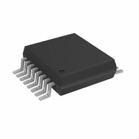
AD5933YRSZ Analog Devices Inc, AD5933YRSZ Datasheet - Page 19

AD5933YRSZ
Manufacturer Part Number
AD5933YRSZ
Description
IC NTWK ANALYZER 12B 1MSP 16SSOP
Manufacturer
Analog Devices Inc
Datasheet
1.AD5933YRSZ.pdf
(44 pages)
Specifications of AD5933YRSZ
Resolution (bits)
12 b
Master Fclk
16.776MHz
Voltage - Supply
2.7 V ~ 5.5 V
Operating Temperature
-40°C ~ 125°C
Mounting Type
Surface Mount
Package / Case
16-SSOP
Supply Voltage Range
2.7V To 5.5V
Operating Temperature Range
-40°C To +125°C
Digital Ic Case Style
SSOP
No. Of Pins
16
Frequency Max
0.1MHz
Termination Type
SMD
Pin Count
16
Screening Level
Automotive
Package Type
SSOP
Filter Terminals
SMD
Rohs Compliant
Yes
Communication Function
Network Analyzer
Lead Free Status / RoHS Status
Lead free / RoHS Compliant
For Use With
EVAL-AD5933EBZ - BOARD EVALUATION FOR AD5933
Tuning Word Width (bits)
-
Lead Free Status / Rohs Status
Compliant
Other names
AD5933BRSZ
Q2204656A
Q2204656A
Available stocks
Company
Part Number
Manufacturer
Quantity
Price
Company:
Part Number:
AD5933YRSZ
Manufacturer:
ADI
Quantity:
5 000
Company:
Part Number:
AD5933YRSZ
Manufacturer:
Fujitsu
Quantity:
500
Part Number:
AD5933YRSZ
Manufacturer:
ADI/亚德诺
Quantity:
20 000
GAIN FACTOR TEMPERATURE VARIATION
IMPEDANCE ERROR
It is important when reading the following section to note that the
output impedance associated with the excitation voltages was
actually measured and then calibrated out for each impedance
error measurement. This was done using a Keithley current
source/sink and measuring the voltage.
R
specification table) is only a typical specification and can vary
from part to part. This method may not be achievable for large
volume applications and in such cases, it is advised to use an extra
low impedance output amplifier, as shown in Figure 4, to improve
accuracy.
The following are examples of the AD5933 performance when
operating in the six different impedance ranges. Note that the
gain factor is calculated with a precision resistor in each case.
In Figure 26 to Figure 31, the 10 kHz excitation frequency was
generated using a 4 MHz clock.
Minimizing the impedance range under testing also optimizes the
AD5933 measurement performance.
Impedance Range 1 (0.1 kΩ to 1 kΩ)
The following conditions were used to conduct the test, as shown in
Figure 26:
The typical impedance error variation with temperature is in the
order of 30 ppm/°C. Figure 25 shows an impedance profile with a
variation in temperature for 100 kΩ impedance using a two-point
gain factor calibration.
Figure 25. Impedance Profile Variation with Temperature Using a Two-Point
OUT
Output excitation voltage = 2 V p-p
Calibration impedance value, Z
PGA gain = ×1
Supply voltage = 3.3 V
Current-to-voltage amplifier gain resistor = 100 Ω
(for example ,200 Ω specified for a 1.98 V p-p in the
101.5
101.0
100.5
100.0
99.5
99.0
98.5
54
VDD = 3.3V
CALIBRATION FREQUENCY = 60kHz
MEASURED CALIBRATION IMPEDANCE = 100kΩ
56
Gain Factor Calibration
58
FREQUENCY (kHz)
60
CALIBRATION
+125°C
+25°C
–40°C
62
= 100 Ω
64
66
Rev. C | Page 19 of 44
Impedance Range 2 (1 kΩ to 10 kΩ)
The following conditions were used to conduct the test, as shown in
Figure 27:
Figure 26. Impedance Range 1 Typical % Impedance Error over Frequency
Figure 27. Impedance Range 2 Typical % Impedance Error over Frequency
Output excitation voltage = 2 V p-p
Calibration impedance value, Z
PGA gain = ×1
Supply voltage = 3.3 V
Current-to-voltage amplifier gain resistor = 1 kΩ
2.0
1.8
1.6
1.4
1.2
1.0
0.8
0.6
0.4
0.2
7
6
5
4
3
2
1
0
0
R
CALIBRATION IMPEDANCE = 100Ω
T
R
CALIBRATION IMPEDANCE = 1kΩ
T
A
FB
A
FB
= 25°C
= 25°C
= 0.1kΩ
10
= 1kΩ
10
FREQUENCY (kHz)
35
FREQUENCY (kHz)
35
CALIBRATION
60
60
= 1 kΩ
5kΩ
10kΩ
100
0.5kΩ
1kΩ
100
AD5933


