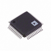
AD9830ASTZ Analog Devices Inc, AD9830ASTZ Datasheet - Page 5

AD9830ASTZ
Manufacturer Part Number
AD9830ASTZ
Description
IC DDS 10BIT 50MHZ CMOS 48-TQFP
Manufacturer
Analog Devices Inc
Datasheet
1.AD9830ASTZ.pdf
(16 pages)
Specifications of AD9830ASTZ
Resolution (bits)
10 b
Master Fclk
50MHz
Tuning Word Width (bits)
32 b
Voltage - Supply
4.75 V ~ 5.25 V
Operating Temperature
-40°C ~ 85°C
Mounting Type
Surface Mount
Package / Case
48-TQFP, 48-VQFP
Pll Type
Direct Digital Synthesis
Frequency
50MHz
Supply Current
60mA
Supply Voltage Range
4.75V To 5.25V
Digital Ic Case Style
TQFP
No. Of Pins
48
Operating Temperature Range
-40°C To +85°C
Ic Function
Direct Digital Synthesizer
Svhc
No SVHC (15-Dec-2010)
Rohs Compliant
Yes
Bandwidth
50MHz
Lead Free Status / RoHS Status
Lead free / RoHS Compliant
For Use With
EVAL-AD9830EBZ - BOARD EVALUATION AD9830
Lead Free Status / RoHS Status
Lead free / RoHS Compliant, Lead free / RoHS Compliant
Available stocks
Company
Part Number
Manufacturer
Quantity
Price
Company:
Part Number:
AD9830ASTZ
Manufacturer:
Analog Devices Inc
Quantity:
10 000
Company:
Part Number:
AD9830ASTZ-REEL
Manufacturer:
Analog Devices Inc
Quantity:
10 000
REV. A
Mnemonic
POWER SUPPLY
AVDD
AGND
DVDD
DGND
ANALOG SIGNAL AND REFERENCE
IOUT, IOUT
FS ADJUST
REFIN
REFOUT
COMP
DIGITAL INTERFACE AND CONTROL
MCLK
FSELECT
WR
D0–D15
A0–A2
PSEL0, PSEL1
SLEEP
RESET
Function
Positive power supply for the analog section. A 0.1 F capacitor should be connected between AVDD and
AGND. AVDD has a value of +5 V
Analog Ground.
Positive power supply for the digital section. A 0.1 F decoupling capacitor should be connected between DVDD
and DGND. DVDD has a value of +5 V
Digital Ground.
Current Output. This is a high impedance current source. A load resistor should be connected between IOUT
and AGND. IOUT should be either tied directly to AGND or through an external load resistor to AGND.
Full-Scale Adjust Control. A resistor (R
nitude of the full-scale DAC current. The relationship between R
Voltage Reference Input. The AD9830 can be used with either the on-board reference, which is available from pin
REFOUT, or an external reference. The reference to be used is connected to the REFIN pin. The AD9830 ac-
cepts a reference of 1.21 V nominal.
Voltage Reference Output. The AD9830 has an on-board reference of value 1.21 V nominal. The reference is
made available on the REFOUT pin. This reference is used as the reference to the DAC by connecting REFOUT
to REFIN. REFOUT should be decoupled with a 10 nF capacitor to AGND.
Compensation pin. This is a compensation pin for the internal reference amplifier. A 10 nF decoupling ceramic
capacitor should be connected between COMP and AVDD.
Digital Clock Input. DDS output frequencies are expressed as a binary fraction of the frequency of MCLK. The
output frequency accuracy and phase noise are determined by this clock.
Frequency Select Input. FSELECT controls which frequency register, FREQ0 or FREQ1, is used in the phase ac-
cumulator. FSELECT is sampled on the rising MCLK edge. FSELECT needs to be in steady state when an
MCLK rising edge occurs. If FSELECT changes value when an MCLK rising edge occurs, there is an uncertainty
of one MCLK cycle as to when control is transferred to the other frequency register. To avoid any uncertainty, a
change on FSELECT should not coincide with an MCLK rising edge.
Write, Edge-Triggered Digital Input. The WR pin is used when writing data to the AD9830. The data is loaded
into the AD9830 on the rising edge of the WR pulse. This data is then loaded into the destination register on the
MCLK rising edge. The WR pulse rising edge should not coincide with the MCLK rising edge as there will be an
uncertainty of one MCLK cycle regarding the loading of the destination register with the new data. The WR ris-
ing edge should occur before an MCLK rising edge. The data will then be transferred into the destination register
on the MCLK rising edge. Alternatively, the WR rising edge can occur after the MCLK rising edge and the desti-
nation register will be loaded on the next MCLK rising edge.
Data Bus, Digital Inputs for destination registers.
Address Digital Inputs. These address bits are used to select the destination register to which the digital data is to
be written.
Phase Select Input. The AD9830 has four phase registers. These registers can be used to alter the value being in-
put to the SIN ROM. The contents of the phase register can be added to the phase accumulator output, the inputs
PSEL0 and PSEL1 selecting the phase register to be used. Like the FSELECT input, the AD9830 samples the
PSEL0 and PSEL1 inputs on the MCLK rising edge. Therefore, these inputs should be in steady state at the
MCLK rising edge or, there is an uncertainty of one MCLK cycle as to when control is transferred to the selected
phase register.
Low Power Control, active low digital input. SLEEP puts the AD9830 into a low power mode. Internal clocks
are disabled and the DAC’s current sources and REFOUT are turned off. The AD9830 is re-enabled by taking
SLEEP high.
Reset, active low digital input. RESET resets the phase accumulator to zero which corresponds to an analog
output of midscale.
V
REFIN
PIN DESCRIPTION
5%.
IOUT
SET
= 1.21 V nominal, R
) is connected between this pin and AGND. This determines the mag-
5%.
FULL-SCALE
–5–
= 16 V
SET
REFIN
SET
= 1 k typical
/R
and the full-scale current is as follows:
SET
AD9830


