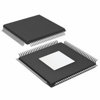
AD9858BSVZ Analog Devices Inc, AD9858BSVZ Datasheet - Page 26

AD9858BSVZ
Manufacturer Part Number
AD9858BSVZ
Description
IC DDS DAC 10BIT 1GSPS 100-TQFP
Manufacturer
Analog Devices Inc
Datasheet
1.AD9858BSVZ.pdf
(32 pages)
Specifications of AD9858BSVZ
Design Resources
Low Jitter Sampling Clock Generator for High Performance ADCs Using AD9958/9858 and AD9515 (CN0109)
Resolution (bits)
10 b
Master Fclk
1GHz
Tuning Word Width (bits)
32 b
Voltage - Supply
3.14 V ~ 3.47 V
Operating Temperature
-40°C ~ 85°C
Mounting Type
Surface Mount
Package / Case
100-TQFP Exposed Pad, 100-eTQFP, 100-HTQFP, 100-VQFP
Pll Type
Frequency Synthesis
Frequency
1GHz
Supply Voltage Range
3.135 To 3.165V, 4.75V To 5.25V
Digital Ic Case Style
TQFP
No. Of Pins
100
Operating Temperature Range
-40°C To +85°C
Lead Free Status / RoHS Status
Lead free / RoHS Compliant
For Use With
AD9858/TLPCBZ - BOARD EVAL TRANSLATION LOOP
Lead Free Status / RoHS Status
Lead free / RoHS Compliant, Lead free / RoHS Compliant
Available stocks
Company
Part Number
Manufacturer
Quantity
Price
Company:
Part Number:
AD9858BSVZ
Manufacturer:
ADI
Quantity:
98
Company:
Part Number:
AD9858BSVZ
Manufacturer:
Analog Devices Inc
Quantity:
10 000
Part Number:
AD9858BSVZ
Manufacturer:
ADI/亚德诺
Quantity:
20 000
AD9858
Profile Selection
A profile consists of a specific group of memory registers (see
Table 6). In the AD9858, each profile contains a 32-bit frequency
tuning word and a 14-bit phase offset word. Each profile is
selectable via two external profile select pins (PS0 and PS1), as
defined in Table 12. The specific mapping of registers to profiles is
detailed in the Register Bit Descriptions section. The user should
be aware that selection of a profile is internally synchronized
with DDS CLK using the SYNCLK timing. That is, SYNCLK is
used to synchronize the assertion of the profile select pins (PS0
and PS1). Therefore, the PS0 and PS1 pins must be set up and
held around the rising edge of SYNCLK.
Table 12.
PS1
0
0
1
1
PS0
0
1
0
1
Profile
0
1
2
3
Rev. C | Page 26 of 32
The profiles are available to the user to provide rapid changing
of device parameters via external hardware, which alleviates the
speed limitations imposed by the I/O port. For example, the user
might preprogram the four phase offset registers with values that
correspond to phase increments of 90°. By controlling the PS0 and
PS1 pins, the user can implement π /2 phase modulation. The data
modulation rate is much higher than that possible by repeatedly
reloading a single phase offset register via the I/O port.


