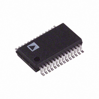
AD9850BRS Analog Devices Inc, AD9850BRS Datasheet

AD9850BRS
Specifications of AD9850BRS
Available stocks
Related parts for AD9850BRS
AD9850BRS Summary of contents
Page 1
FEATURES 125 MHz Clock Rate On-Chip High Performance DAC and High Speed Comparator DAC SFDR > MHz A 32-Bit Frequency Tuning Word Simplified Control Interface: Parallel Byte or Serial Loading Format Phase Modulation Capability 3.3 ...
Page 2
... IV 25°C I 25°C IV Full VI Full VI Full VI Full VI 25°C V 25°C V 25°C V 25°C V 25°C V 25°C IV –2– AD9850BRS Min Typ Max Unit 1 125 MHz 1 110 MHz 3.2 ns 4.1 ns 10.24 mA 20.48 mA –10 + 150 ppm/°C µ nA/° ...
Page 3
... Unit 3.5 V 2.4 V 0.8 V µA 12 µ 100 160 mW 155 200 mW 220 320 mW 380 480 AD9850BRS Min Typ Max Unit 3.5 ns 3.5 ns 3.5 ns 3.5 ns 7.0 ns 3.5 ns 7 CLKIN Cycles 13 CLKIN Cycles 7.0 ns 3 CLKIN Cycles 13 CLKIN Cycles 2 CLKIN Cycles µs 5 ...
Page 4
... Model Temperature Range AD9850BRS –40°C to +85°C AD9850BRS-REEL –40°C to +85°C AD9850BRSZ* –40°C to +85°C AD9850BRSZ-REEL* –40°C to +85°C AD9850/CGPCB AD9850/FSPCB *Z = Pb-free part. EXPLANATION OF TEST LEVELS Test Level I 100% Production Tested. III Sample Tested Only. ...
Page 5
Pin No. Mnemonic Function 8-Bit Data Input. This is the 8-bit data port for iteratively loading the 32-bit frequency and the 8-bit phase control word MSB LSB. ...
Page 6
AD9850–Typical Performance Characteristics Spectrum CH1 S 10dB/REF –8.6dBm CLOCK 125MHz AD9850 0 RBW # 100Hz VBW 100Hz ATN # 30dB SWP START 0Hz TPC 1. SFDR, CLKIN = 125 MHz/f CH1 S Spectrum –10dBm 10dB/REF CLOCK 125MHz AD9850 0 RBW ...
Page 7
Tek Run: 50.0GS/s ET Average 1 Ch1 1.00V TPC 7. Comparator Output Rise Time (5 V Supply/15 pF Load 3. CLKIN – MHz ...
Page 8
AD9850 +V GND S IOUT 8-b 5 PARALLEL DATA, OR 1-b 40 SERIAL DATA, DATA PROCESSOR RESET, AND 2 BUS CLOCK LINES AD9850 IOUTB VINN XTAL CLK VINP OSC QOUT QOUTB RSET Figure 1. Basic AD9850 Clock Generator Application with ...
Page 9
N ACCUMULATOR TUNING WORD SPECIFIES OUTPUT FREQUENCY AS A FRACTION OF REF CLOCK FREQUENCY Figure 4. Basic DDS Block Diagram and Signal Flow of AD9850 AD9850 is a sampled signal, its output spectrum follows the Nyquist sampling theorem. Specifically, its ...
Page 10
AD9850 Table II. Factory Reserved Internal Test Control Codes W0* DATA CLK FQ UD CLKIN COS OUT *OUTPUT UPDATE CAN OCCUR AFTER ANY WORD LOAD AND IS ASYNCHRONOUS WITH THE REFERENCE CLOCK Figure 6. Parallel ...
Page 11
CLKIN RESET COS OUT NOTE: THE TIMING DIAGRAM ABOVE SHOWS THE MINIMAL AMOUNT OF RESET TIME NEEDED BEFORE WRITING TO THE DEVICE. HOWEVER, THE MASTER RESET DOES NOT HAVE TO BE SYNCHRONOUS WITH THE CLKIN IF THE MINIMAL TIME IS ...
Page 12
... Freq-b9 W10 Freq-b10 W11 Freq-b11 W12 Freq-b12 W13 Freq-b13 XXXXX011 DATA (SERIAL) W32 = 0 NOTE: W32 AND W33 SHOULD ALWAYS BE SET TO 0. ENABLE SERIAL MODE Figure 10. Serial Load Enable Sequence 2 AD9850BRS 3 +V SUPPLY CLK CYCLES W14 Freq-b14 W15 Freq-b15 W16 Freq-b16 W17 ...
Page 13
DATA (7) – CLK V CC IOUT IOUTB DAC Output Comparator Output PCB LAYOUT INFORMATION The AD9850/CGPCB and AD9850/FSPCB evaluation boards (Figures 15 through 18) represent typical implementations of the AD9850 and exemplify the use of high ...
Page 14
AD9850 AD9850 Evaluation Board Instructions Required Hardware/Software • IBM compatible computer operating in a Windows environment. • Printer port, 3.5 inch floppy drive, and Centronics compatible printer cable. • XTAL clock or signal generator—if using a signal generator, dc offset ...
Page 15
... C5 0.1 F 0.1 F 0 Figure 15. AD9850/FSPCB Electrical Schematic AD9850BRS (28-Lead SSOP) 74HCT574 H-CMOS Octal Flip-Flop 0.1 µF Ceramic Chip Capacitor 10 µF Tantalum Chip Capacitor 3.9 kΩ Resistor 50 Ω Resistor 2.2 kΩ Resistor 25 Ω Resistor 1 kΩ Resistor 36-Pin D Connector Banana Jack BNC Connector – ...
Page 16
AD9850 16a. AD9850/FSPCB Top Layer 16b. AD9850/FSPCB Ground Plane Figure 16. AD9850/FSPCB Evaluation Board Layout 16c. AD9850/FSPCB Power Plane 16d. AD9850/FSPCB Bottom Layer –16– REV. H ...
Page 17
... CHECK 33 CLK 34 35 STROBE 36 STROBE COMPONENT LIST Integrated Circuits U1 AD9850BRS (28-Lead SSOP) U2, U3 74HCT574 H-CMOS Octal Flip-Flop Capacitors C1 470 pF Ceramic Chip Capacitor 0.1 µF Ceramic Chip Capacitor C10 10 µF Tantalum Chip Capacitor C6, C7 C11 22 pF Ceramic Chip Capacitor C12 3 ...
Page 18
AD9850 18a. AD9850/CGPCB Top Layer 18b. AD9850/CGPCB Ground Plane Figure 18. AD9850/CGPCB Evaluation Board Layout 18c. AD9850/CGPCB Power Plane 18d. AD9850/CGPCB Bottom Layer –18– REV. H ...
Page 19
MAX 0.05 MIN REV. H OUTLINE DIMENSIONS 28-Lead Shrink Small Outline Package [SSOP] (RS-28) Dimensions shown in millimeters 10.50 10.20 9. 5.60 8.20 5.30 7.80 5.00 7. 1.85 1.75 0.10 COPLANARITY 1.65 0.25 0.09 0.65 ...
Page 20
AD9850 Revision History Location 2/04—Data Sheet changed from REV REV. H. Changes to SPECIFICATIONS . . . . . . . . . . . . . . . . . . . . . . . . ...


