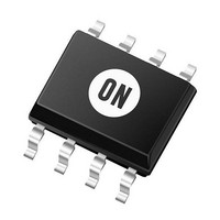
LM317LBDR2 ON Semiconductor, LM317LBDR2 Datasheet - Page 7

LM317LBDR2
Manufacturer Part Number
LM317LBDR2
Description
Linear Regulators - Standard 100mA ADJ 1.2-37V
Manufacturer
ON Semiconductor
Datasheet
1.LM317LD.pdf
(12 pages)
Specifications of LM317LBDR2
Polarity
Positive
Number Of Outputs
1
Output Type
Adjustable
Output Voltage
1.2 V to 37 V
Output Current
0.1 A
Line Regulation
0.07 % / V
Load Regulation
0.5 %
Input Voltage Max
40 V
Maximum Operating Temperature
+ 125 C
Minimum Operating Temperature
- 40 C
Package / Case
SOIC-8
Mounting Style
SMD/SMT
Reference Voltage
1.3 V
Voltage Regulation Accuracy
4 %
Lead Free Status / Rohs Status
Lead free / RoHS Compliant
Available stocks
Company
Part Number
Manufacturer
Quantity
Price
Part Number:
LM317LBDR2
Manufacturer:
ON/安森美
Quantity:
20 000
Company:
Part Number:
LM317LBDR2G
Manufacturer:
ON
Quantity:
20 000
Part Number:
LM317LBDR2G
Manufacturer:
ON
Quantity:
20 000
Basic Circuit Operation
operation, the LM317L develops and maintains a nominal
1.25 V reference (V
terminals. This reference voltage is converted to a
programming current (I
constant current flows through R
output voltage is given by:
represents an error term in the equation, the LM317L was
designed to control I
constant. To do this, all quiescent operating current is
returned to the output terminal. This imposes the
requirement for a minimum load current. If the load current
is less than this minimum, the output voltage will rise.
voltage differential across the circuit which is important to
performance, and operation at high voltages with respect to
ground is possible.
The LM317L is a 3-terminal floating regulator. In
Since the current from the adjustment terminal (I
Since the LM317L is a floating regulator, it is only the
-0.5
-1.0
-1.5
1.5
1.0
0.5
1.0
0.5
0
0
Figure 18. Basic Circuit Configuration
V
in
V
0
ref
V
Adjust
= 1.25 V Typical
Figure 16. Line Transient Response
V
I
T
L
out
out
J
= 50 mA
= 25°C
LM317L
= 10 V
= V
ref
Adj
) between its output and adjustment
I
Adj
PROG
ref
10
to less than 100 mA and keep it
(1 +
) by R
t, TIME (ms)
V
V
R
R
ref
out
2
2
1
20
1
to ground. The regulated
) + I
(see Figure 13), and this
+
C
C
L
Adj
Adj
R
= 1.0 mF;
R
I
2
= 10 mF
1
V
PROG
R
in
APPLICATIONS INFORMATION
2
30
C
Without C
V
L
out
= 0;
LM317L, NCV317LB
http://onsemi.com
Adj
40
Adj
)
7
Load Regulation
regulation, but a few precautions are needed to obtain
maximum performance. For best performance, the
programming resistor (R1) should be connected as close to
the regulator as possible to minimize line drops which
effectively appear in series with the reference, thereby
degrading regulation. The ground end of R2 can be returned
near the load ground to provide remote ground sensing and
improve load regulation.
External Capacitors
(C
impedance.
improve ripple rejection. This capacitor (C
ripple from being amplified as the output voltage is
increased. A 10 mF capacitor should improve ripple
rejection about 15 dB at 120 Hz in a 10 V application.
capacitance, like any feedback circuit, certain values of
external capacitance can cause excessive ringing. An output
capacitance (C
aluminum electrolytic capacitor on the output swamps this
effect and insures stability.
The LM317L is capable of providing extremely good load
A 0.1 mF disc or 1.0 mF tantalum input bypass capacitor
The adjustment terminal may be bypassed to ground to
Although the LM317L is stable with no output
-0.1
-0.2
-0.3
in
100
0.3
0.2
0.1
50
) is recommended to reduce the sensitivity to input line
0
0
C
L
= 1 mF; C
0
Figure 17. Load Transient Response
O
) in the form of a 1.0 mF tantalum or 25 mF
Adj
C
= 10 mF
L
10
= 0.3 mF; C
t, TIME (ms)
Adj
20
= 10 mF
30
I
L
V
V
I
T
NL
out
J
in
Adj
= 25°C
= 15 V
= 50 mA
= 10 V
) prevents
40


