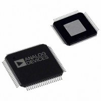
AD9852ASVZ Analog Devices Inc, AD9852ASVZ Datasheet - Page 22

AD9852ASVZ
Manufacturer Part Number
AD9852ASVZ
Description
IC DDS SYNTHESIZER CMOS 80-TQFP
Manufacturer
Analog Devices Inc
Datasheet
1.AD9852ASTZ.pdf
(52 pages)
Specifications of AD9852ASVZ
Resolution (bits)
12 b
Master Fclk
300MHz
Tuning Word Width (bits)
48 b
Voltage - Supply
3.14 V ~ 3.47 V
Operating Temperature
-40°C ~ 85°C
Mounting Type
Surface Mount
Package / Case
80-TQFP Exposed Pad, 80-eTQFP, 80-HTQFP, 80-VQFP
Transmitting Current
815mA
Rf Ic Case Style
TQFP
No. Of Pins
80
Supply Voltage Range
3.135V To 3.465V
Operating Temperature Range
-40°C To +85°C
Msl
MSL 3 - 168 Hours
Frequency Max
300MHz
Lead Free Status / RoHS Status
Lead free / RoHS Compliant
For Use With
AD9852/PCBZ - BOARD EVAL FOR AD9852
Lead Free Status / Rohs Status
Compliant
Available stocks
Company
Part Number
Manufacturer
Quantity
Price
Company:
Part Number:
AD9852ASVZ
Manufacturer:
ADI
Quantity:
263
Company:
Part Number:
AD9852ASVZ
Manufacturer:
Analog Devices Inc
Quantity:
10 000
Part Number:
AD9852ASVZ
Manufacturer:
ADI/亚德诺
Quantity:
20 000
AD9852
Additional flexibility in the ramped FSK mode is provided by
the AD9852’s ability to respond to changes in the 48-bit delta
frequency word and/or the 20-bit ramp rate counter at any time
during the ramping from F1 to F2 or vice versa. To create these
nonlinear frequency changes, it is necessary to combine several
linear ramps with different slopes in a piecewise fashion. This is
done by programming and executing a linear ramp at a rate or
slope and then altering the slope (by changing the ramp rate
clock or delta frequency word, or both). Changes in slope can
be made as often as needed before the destination frequency has
been reached to form the desired nonlinear frequency sweep
response. These piecewise changes can be precisely timed using
the 32-bit internal update clock (see the Internal and External
Update Clock section).
Nonlinear ramped FSK has the appearance of the chirp function
shown in Figure 41. The major difference between a ramped
FSK function and a chirp function is that FSK is limited to
operation between F1 and F2, whereas chirp operation has no
F2 limit frequency.
Two additional control bits (CLR ACC1 and CLR ACC2) are
available in the ramped FSK mode that allow more options. Setting
CLR ACC1 (Register Address 1F hex) high clears the 48-bit
frequency accumulator (ACC1) output with a retriggerable
one-shot pulse of one system clock duration. If the CLR ACC1
bit is left high, a one-shot pulse is delivered on the rising edge of
every update clock. The effect is to interrupt the current ramp,
reset the frequency to the start point (F1 or F2), and then
continue to ramp up (or down) at the previous rate. This occurs
I/O UD CLK
FSK DATA
MODE
TW1
TW2
FREQUENCY
000 (DEFAULT)
F2
F1
0
0
0
Figure 39. Effect of Premature Ramped FSK Data
Rev. E | Page 22 of 52
010 (RAMPED FSK)
F1
F2
even when a static F1 or F2 destination frequency has been
achieved.
Alternatively, the CLR ACC2 control bit (Register Address 1F hex)
can be used to clear both the frequency accumulator (ACC1)
and the phase accumulator (ACC2). When this bit is set high,
the output of the phase accumulator results in 0 Hz output from
the DDS. As long as this bit is set high, the frequency and phase
accumulators are cleared, resulting in 0 Hz output. To return to
previous DDS operation, CLR ACC2 must be set to logic low.
CHIRP (MODE 011)
Chirp mode is also known as pulsed FM. Most chirp systems
use a linear FM sweep pattern, but the AD9852 can also support
nonlinear patterns. In radar applications, use of chirp or pulsed
FM allows operators to significantly reduce the output power
needed to achieve the same result a single frequency radar
system produces. Figure 41 represents a very low resolution
nonlinear chirp that demonstrates the different slopes created
by varying the time steps (ramp rate) and frequency steps (delta
frequency word).
The AD9852 permits precise, internally generated linear,
or externally programmed nonlinear, pulsed or continuous
FM over the complete frequency range, duration, frequency
resolution, and sweep direction(s). All of these options are user
programmable. A block diagram of the FM chirp components
is shown in Figure 40.


