AD9957BSVZ Analog Devices Inc, AD9957BSVZ Datasheet - Page 25
AD9957BSVZ
Manufacturer Part Number
AD9957BSVZ
Description
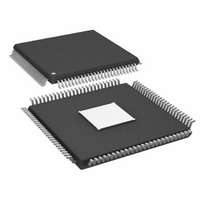
IC DDS 1GSPS 14BIT IQ 100TQFP
Manufacturer
Analog Devices Inc
Datasheet
1.AD9957BSVZ-REEL.pdf
(64 pages)
Specifications of AD9957BSVZ
Resolution (bits)
14 b
Master Fclk
1GHz
Tuning Word Width (bits)
32 b
Voltage - Supply
1.8V, 3.3V
Operating Temperature
-40°C ~ 85°C
Mounting Type
Surface Mount
Package / Case
100-TQFP Exposed Pad, 100-eTQFP, 100-HTQFP, 100-VQFP
Frequency Range
60MHz To 1GHz
Rf Type
Quadrature
Supply Voltage Range
1.71V To 1.89V, 3.135V To 3.465
Rf Ic Case Style
TQFP
No. Of Pins
100
Operating Temperature Range
-40°C To +85°C
Operating Temperature (max)
85C
Operating Temperature (min)
-40C
Pin Count
100
Mounting
Surface Mount
Case Height
1mm
Screening Level
Industrial
Lead Free Status / RoHS Status
Lead free / RoHS Compliant
For Use With
AD9957/PCBZ - BOARD EVAL AD9957 QUADRATURE MOD
Lead Free Status / Rohs Status
Compliant
Available stocks
Company
Part Number
Manufacturer
Quantity
Price
Company:

Part Number:
AD9957BSVZ
Manufacturer:
AD
Quantity:
1 200
Company:
Part Number:
AD9957BSVZ
Manufacturer:
Analog Devices Inc
Quantity:
10 000
Part Number:
AD9957BSVZ
Manufacturer:
ADI/亚德诺
Quantity:
20 000
Company:
Part Number:
AD9957BSVZ-REEL
Manufacturer:
Analog Devices Inc
Quantity:
10 000
Part Number:
AD9957BSVZ-REEL
Manufacturer:
ADI/亚德诺
Quantity:
20 000


QUADRATURE MODULATOR
The digital quadrature modulator stage shifts the frequency of
the baseband spectrum of the incoming data stream up to the
desired carrier frequency (a process known as upconversion).
At this point, the baseband data, which was delivered to the
device at an I/Q sample rate of f
equal to the frequency of SYSCLK, making the data sampling
rate equal to the sampling rate of the carrier signal.
The frequency of the carrier signal is controlled by a direct
digital synthesizer (DDS). The DDS very precisely generates the
desired carrier frequency from the internal reference clock
(SYSCLK). The carrier is applied to the I and Q multipliers in
quadrature fashion (90° phase offset) and summed, yielding a
data stream that represents the quadrature modulated carrier.
The modulation is performed digitally, avoiding the phase
offset, gain imbalance, and crosstalk issues commonly associated
with analog modulators. Note that the modulated, so-called
signal is a number stream sampled at the rate of SYSCLK, the
same rate at which the DAC is clocked.
The orientation of the modulated signal with respect to the
carrier is controlled by a spectral invert bit. This bit resides in
each of the eight profile registers. By default, the time domain
output of the quadrature modulator takes the form
When the spectral invert bit is asserted, it becomes
DDS CORE
The direct digital synthesizer (DDS) block generates sine
and/or cosine signals. In single tone mode, the DDS generates
either a digital sine or cosine waveform based on the select DDS
sine output bit. In QDUC mode, the DDS generates the quadra-
ture carrier reference signal that digitally modulates the I/Q
baseband signal.
The DDS output frequency is tuned using registers accessed via
the serial I/O port. This allows for both precise tuning and
instantaneous changing of the carrier frequency.
The equation relating output frequency (f
frequency tuning word (FTW) and the system clock (f
where FTW is a decimal number from 0 to 2,147,483,647 (2
Solving for FTW yields
I(t) × cos(ωt) − Q(t) × sin(ωt)
I(t) × cos(ωt) + Q(t) × sin(ωt)
FTW
f
OUT
=
=
round
FTW
2
32
2
f
32
SYSCLK
f
SYSCLK
f
OUT
IQ
, has been upsampled to a rate
OUT
) of the DDS to the
SYSCLK
31
− 1).
) is
Rev. B | Page 25 of 64
(2)
(3)
(4)
(5)
where the round() function means to round the result to the
nearest integer. For example, for f
122.88 MHz, then FTW = 1,433,053,867 (0x556AAAAB).
In single tone mode, the DDS frequency, phase, and amplitude
are all programmable via the serial I/O port. The amplitude
is controlled by means of a digital multiplier using a 14-bit
fractional scale value called the amplitude scale factor (ASF).
The LSB weight is 2
0.99993896484375 (1 − 2
program the appropriate control register bit (see the details of
CFR2<24> in the Register Bit Descriptions section). When
bypassed, the ASF multiplier clocks are disabled to conserve
power. The phase offset is controlled by means of a digital adder
that uses a 14-bit offset value called the phase offset word (POW).
The adder is situated between the phase accumulator and the
angle-to-amplitude conversion logic in the DDS core. The adder
applies the POW to the instantaneous phase values produced by
the DDS phase accumulator. The adder is MSB aligned with the
phase accumulator yielding an LSB weight of 2
a resolution of ~0.022° or ~0.000383 radians). Both the ASF and
the POW are available for each of the eight profiles.
INVERSE SINC FILTER
The sampled carrier data stream is the input to the digital-to-
analog converter. The DAC output spectrum is shaped by the
characteristic sin(x)/x (or sinc) envelope, due to the intrinsic
zero-order hold effect associated with DAC-generated signals.
The shape of the sinc envelope is well known and can be
compensated for. This compensation is provided by the inverse
sinc filter preceding the DAC.
The inverse sinc filter is implemented as a digital FIR filter. Its
response characteristic very nearly matches the inverse of the
sinc envelope, as shown in Figure 37 (along with the sinc
envelope for comparison).
The inverse sinc filter is enabled through a bit in the register
map. The filter tap coefficients are listed in Table 4. The filter
predistorts the data prior to its arrival at the DAC to compensate
for the sinc envelope that otherwise distorts the spectrum.
When the inverse sinc filter is enabled, it introduces a ~3.0 dB
insertion loss. The inverse sinc compensation is effective for
output frequencies up to 40% (nominally) of the DAC sample rate.
Table 4. Inverse Sinc Filter Tap Coefficients
Tap No.
1
2
3
4
Tap Value
−35
+134
−562
+6729
−14
, yielding a multiplier range of 0 to
−14
). To bypass the ASF multiplier,
OUT
= 41 MHz and f
−14
(which equates to
Tap No.
7
6
5
4
AD9957
SYSCLK
=
Related parts for AD9957BSVZ
Image
Part Number
Description
Manufacturer
Datasheet
Request
R

Part Number:
Description:
D/A Converter Evaluation Board
Manufacturer:
Analog Devices Inc
Datasheet:


Part Number:
Description:
±1.7g Dual-Axis IMEMS Accelerometer Evaluation Board
Manufacturer:
Analog Devices Inc
Datasheet:

Part Number:
Description:
Inertial Sensor Evaluation System
Manufacturer:
Analog Devices Inc
Datasheet:
Part Number:
Description:
Manufacturer:
Analog Devices Inc
Datasheet:
Part Number:
Description:
Manufacturer:
Analog Devices Inc
Datasheet:
Part Number:
Description:
Manufacturer:
Analog Devices Inc
Datasheet:
Part Number:
Description:
Manufacturer:
Analog Devices Inc
Datasheet:
Part Number:
Description:
Manufacturer:
Analog Devices Inc
Datasheet:
Part Number:
Description:
Manufacturer:
Analog Devices Inc
Datasheet:
Part Number:
Description:
Manufacturer:
Analog Devices Inc
Datasheet:
Part Number:
Description:
Manufacturer:
Analog Devices Inc
Datasheet:
Part Number:
Description:
Manufacturer:
Analog Devices Inc
Datasheet: