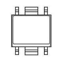
S-1172B33-E6T1G Seiko Instruments, S-1172B33-E6T1G Datasheet - Page 14

S-1172B33-E6T1G
Manufacturer Part Number
S-1172B33-E6T1G
Description
Low Dropout (LDO) Regulators Linear LDO reg Hi 70uA Iq 1000mA Iout
Manufacturer
Seiko Instruments
Datasheet
1.S-1172B18-E6T1G.pdf
(35 pages)
Specifications of S-1172B33-E6T1G
Polarity
Positive
Input Voltage Max
6 V
Output Voltage
3.3 V
Output Type
Fixed
Dropout Voltage (max)
3 V at 300 mA
Output Current
1000 mA
Load Regulation
15 mV
Voltage Regulation Accuracy
1 %
Maximum Power Dissipation
1900 mW
Maximum Operating Temperature
+ 85 C
Mounting Style
SMD/SMT
Package / Case
HSOP-6
Lead Free Status / Rohs Status
Lead free / RoHS Compliant
Available stocks
Company
Part Number
Manufacturer
Quantity
Price
Part Number:
S-1172B33-E6T1G
Manufacturer:
SEIKO/精工
Quantity:
20 000
14
HIGH RIPPLE-REJECTION LOW DROPOUT HIGH OUTPUT CURRENT CMOS VOLTAGE REGULATOR
S-1172 Series
Operation
1. Basic operation
2. Output transistor
Figure 13 shows the block diagram of the S-1172 Series.
The error amplifier compares the reference voltage (V
feedback resistors R
is not influenced by the input voltage and temperature change, to the output transistor.
In the S-1172 Series, a low on-resistance P-channel MOS FET is used as the output transistor.
Be sure that V
current which flows, because of a parasitic diode between the VIN and VOUT pin, when the potential of V
became higher than V
OUT
VIN
VSS
*1. Parasitic diode
does not exceed V
Current
s
supply
Reference voltage
IN
and R
.
V
ref
circuit
f
. It supplies the gate voltage necessary to maintain the constant output voltage which
IN
Error amplifier
+ 0.3 V to prevent the voltage regulator from being damaged due to inverse
−
+
Seiko Instruments Inc.
Figure 13
ref
) with V
fb
, which is the output voltage resistance-divided by
V
R
R
fb
f
s
*1
VOUT
Rev.2.0
_00
OUT


