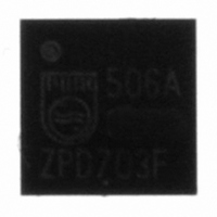
ISP1506ABS ST-Ericsson Inc, ISP1506ABS Datasheet - Page 23

ISP1506ABS
Manufacturer Part Number
ISP1506ABS
Description
IC ULPI TRANSCEIVER 24-HVQFN
Manufacturer
ST-Ericsson Inc
Type
Transceiverr
Datasheet
1.ISP1506ABS.pdf
(79 pages)
Specifications of ISP1506ABS
Number Of Drivers/receivers
1/1
Protocol
USB 2.0
Voltage - Supply
1.65 V ~ 3.6 V
Mounting Type
Surface Mount
Package / Case
24-VQFN Exposed Pad, 24-HVQFN, 24-SQFN, 24-DHVQFN
Lead Free Status / RoHS Status
Lead free / RoHS Compliant
Other names
568-3156
Available stocks
Company
Part Number
Manufacturer
Quantity
Price
Company:
Part Number:
ISP1506ABS
Manufacturer:
ST-Ericsson Inc
Quantity:
1 961
Company:
Part Number:
ISP1506ABS
Manufacturer:
IDT
Quantity:
152
Part Number:
ISP1506ABSUM
Manufacturer:
ST-ERICS
Quantity:
20 000
NXP Semiconductors
ISP1506A_ISP1506B_1
Product data sheet
Fig 7. Interface behavior with respect to RESET_N
DATA[3:0]
RESET_N
CLOCK
NXT
STP
DIR
9.3.2 Interface behavior with respect to RESET_N
9.4.1 Driving 5 V on V
9.4 V
Hi-Z (input)
Hi-Z (input)
The interface protect feature prevents unwanted activity of the ISP1506 whenever the
ULPI interface is not correctly driven by the link. For example, when the link powers up
more slowly than the ISP1506.
The interface protect feature can be disabled by setting the INTF_PROT_DIS bit to logic 1.
The use of the RESET_N pin is optional. When RESET_N is asserted (LOW), the
ISP1506 will assert DIR. All logic in the ISP1506 will be reset, including the analog
circuitry and ULPI registers. During reset, the link must drive DATA[3:0] and STP to LOW;
otherwise undefined behavior may result. When RESET_N is de-asserted (HIGH), the
DIR output will de-assert (LOW) four or five clock cycles later.
interface behavior when RESET_N is asserted (LOW), and subsequently de-asserted
(HIGH). If RESET_N is not used, it must be connected to V
The ISP1506 provides a built-in charge pump. To enable the charge pump, the link must
set the DRV_VBUS bit in the OTG Control register.
The ISP1506 also supports external 5 V supplies. The ISP1506 can control the external
supply using the active-LOW PSW_N open-drain output pin. To enable the external supply
by driving PSW_N to LOW, the link must set the DRV_VBUS_EXT bit in the OTG Control
register to logic 1. The link can optionally set both the DRV_VBUS and DRV_VBUS_EXT
bits to logic 1 to enable the external supply.
Table 8
BUS
power and fault detection
summarizes settings to drive 5 V on V
Hi-Z (link must drive)
Hi-Z (link must drive)
BUS
Rev. 01 — 30 May 2007
Hi-Z (input)
Hi-Z (input)
ISP1506A; ISP1506B
BUS
.
ULPI HS USB OTG transceiver
CC(I/O)
Figure 7
.
© NXP B.V. 2007. All rights reserved.
shows the ULPI
004aaa890
23 of 79


