MIC5841YN Micrel Inc, MIC5841YN Datasheet - Page 5
MIC5841YN
Manufacturer Part Number
MIC5841YN
Description
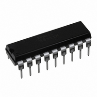
IC DRVR LATCH 8BIT SER IN 18DIP
Manufacturer
Micrel Inc
Type
Driverr
Datasheet
1.MIC5841YN.pdf
(8 pages)
Specifications of MIC5841YN
Number Of Drivers/receivers
8/0
Voltage - Supply
5V
Mounting Type
Through Hole
Package / Case
18-DIP (0.300", 7.62mm)
Lead Free Status / RoHS Status
Lead free / RoHS Compliant
Protocol
-
Other names
576-1307
Available stocks
Company
Part Number
Manufacturer
Quantity
Price
Company:

Part Number:
MIC5841YN
Manufacturer:
ACTEL
Quantity:
144
Part Number:
MIC5841YN
Manufacturer:
MICREL/麦瑞
Quantity:
20 000


Timing Conditions
(TA = 25°C Logic Levels are V
A. Minimum Data Active Time Before Clock Pulse (Data Set-Up Time)...................................................................... 75 ns
B. Minimum Data Active Time After Clock Pulse (Data Hold Time) ............................................................................ 75 ns
C. Minimum Data Pulse Width ................................................................................................................................... 150 ns
D. Minimum Clock Pulse Width................................................................................................................................... 150 ns
E. Minimum Time Between Clock Activation and Strobe ........................................................................................... 300 ns
F. Minimum Strobe Pulse Width.................................................................................................................................. 100 ns
G. Typical Time Between Strobe Activation and Output Transition............................................................................ 500 ns
SERIAL DATA present at the input is transferred to the shift register on the logic “0” to logic “1” transition of the CLOCK
input pulse. On succeeding CLOCK pulses, the registers shift data information towards the SERIAL DATA OUTPUT. The
SERIAL DATA must appear at the input prior to the rising edge of the CLOCK input waveform.
Information present at any register is transferred to its respective latch when the STROBE is high (serial-to-parallel
conversion). The latches will continue to accept new data as long as the STROBE is held high. Applications where the
latches are bypassed (STROBE tied high) will require that the ENABLE input be high during serial data entry.
When the ENABLE input is high, all of the output buffers are disabled (OFF) without affecting information stored in the
latches or shift register. With the ENABLE input low, the outputs are controlled by the state of the latches.
MIC5840 Family Truth Table
L = Low Logic Level
H = High Logic Level
X = Irrelevant
P = Present State
R = Previous State
Micrel, Inc.
May 2006
Serial
Input
Data
H
X
L
Clock
Input
R1
P1
Shift Register Contents
H
I
X
L
1
R1
R1
R2
P2
I
X
2
R2
R2
R3
P3
I
X
3
DD
and V
…
…
…
…
…
…
R7
R7
R8
P8
SS
I
X
8
)
Output
Serial
Data
R7
R7
R8
P8
X
Strobe
Input
H
L
5
R1
P1
I
X
1
Latch Contents
R2
P2
I
X
2
R3
P3
I
X
3
…
…
…
…
R8
P8
I
X
8
Output
Enable
H
L
P1
H
I
1
Output Contents
P2
H
I
2
(408) 955-1690
M9999-050506
MIC5841/42
P3
I
H
3
V
DD
…
… P8
…
= 5V
I
H
8
Related parts for MIC5841YN
Image
Part Number
Description
Manufacturer
Datasheet
Request
R

Part Number:
Description:
Manufacturer:
Micrel Inc
Datasheet:
Part Number:
Description:
Manufacturer:
Micrel Inc
Datasheet:
Part Number:
Description:
Manufacturer:
Micrel Inc
Datasheet:
Part Number:
Description:
Manufacturer:
Micrel Inc
Datasheet:
Part Number:
Description:
Manufacturer:
Micrel Inc
Datasheet:
Part Number:
Description:
Manufacturer:
Micrel Inc
Datasheet:
Part Number:
Description:
Manufacturer:
Micrel Inc
Datasheet:
Part Number:
Description:
Manufacturer:
Micrel Inc
Datasheet:
Part Number:
Description:
Manufacturer:
Micrel Inc
Datasheet:
Part Number:
Description:
Manufacturer:
Micrel Inc
Datasheet:
Part Number:
Description:
Manufacturer:
Micrel Inc
Datasheet:
Part Number:
Description:
Manufacturer:
Micrel Inc
Datasheet:
Part Number:
Description:
Manufacturer:
Micrel Inc
Datasheet:
Part Number:
Description:
Manufacturer:
Micrel Inc
Datasheet: