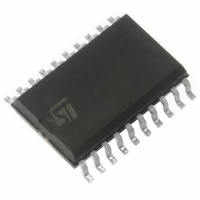
L6374FP013TR STMicroelectronics, L6374FP013TR Datasheet - Page 9

L6374FP013TR
Manufacturer Part Number
L6374FP013TR
Description
IC LINE DRIVER IND QUAD 20SOIC
Manufacturer
STMicroelectronics
Type
Driverr
Datasheet
1.L6374FP013TR.pdf
(19 pages)
Specifications of L6374FP013TR
Number Of Drivers/receivers
4/0
Voltage - Supply
10.8 V ~ 35 V
Mounting Type
Surface Mount
Package / Case
20-SOIC (7.5mm Width)
Supply Voltage (max)
35 V
Supply Voltage (min)
10.8 V
Maximum Operating Temperature
+ 85 C
Mounting Style
SMD/SMT
Minimum Operating Temperature
- 25 C
Supply Current
5000 uA
Lead Free Status / RoHS Status
Lead free / RoHS Compliant
Protocol
-
Lead Free Status / Rohs Status
Details
Other names
497-4012-2
Available stocks
Company
Part Number
Manufacturer
Quantity
Price
L6374
7
8
9
Diagnostic logic
The situations that are monitored and signalled with the Diag output pin are:
●
●
●
Programmable delay
The current limiting circuits can be requested to perform even in absence of a real fault
condition, for a short period, if the load is of capacitive nature or if it is a filament lamp (that
exhibits a very low resistance during the initial heating phase). To avoid the forwarding of
misleading, short diagnostic pulses in coincidence with the intervention of the current
limiting circuits when operating on capacitive loads, a delay of about 5 µs is inserted on the
signal path, between the "OR" of the current limit signals and its use as external diagnostic.
It takes about 1µs to charge (or discharge) by 24 V a capacitor of 5 nF with a current of
120 mA . To implement longer delays (from the intervention of one of the current limiting
circuits to the activation of the diagnostic) an external capacitor can be connected between
pin C3 and ground (pin C3 is otherwise left open).
The delay shall then be determined by the ratio of about 10 pF/µs, using the value of the
capacitance connected to the pin.
Analog inputs (I1,I2,I3,I4)
The input stage of each channel is a high im-pedence comparator with built-in hysteresis
(200 mV) for high noise immunity. Each comparator has one input connected to all the
others and tied to a common pin Ref (Pin 11). If this pin is left floating an internal precise
band gap voltage reference (1.25 V) is applied, otherwise these inputs can be externally
programmed by connecting an external voltage source (from 0 to 5 V) and the current on
this pin is internally limited to ±20 mA. The other input pin of each comparator can swing
from -7 to 35 V.
For this reason it has been implemented the structure shown in
device can also be used as line receiver.
When the input voltage is negative, the current is internally limited by a 15 kΩ resistor as
shown in
subtracting half of the hysteresis to the voltage of pin Ref (see
current limit (OVC) in action; there are 8 individual current limiting circuits, two per each
output, i.e. one per every output transistor; they limit the current that can be either sour-
ced or sunk from each output, to a typical value of 150 mA, equal for all of them;
undervoltage protection (UV);
overtemperature protection (OVP); The diagnostic signal is transmitted via an open
drain output (for ease of wired-or connection of several such signals) and a low level
represents the presence of at least one of the monitored conditions, mentioned above.
Figure 4 on page
10. High and low input thresholds can be obtained by adding and
Figure 5 on page
Figure 4 on page 10
Diagnostic logic
10).
and the
9/19


