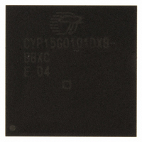
CYP15G0101DXB-BBXC Cypress Semiconductor Corp, CYP15G0101DXB-BBXC Datasheet - Page 10

CYP15G0101DXB-BBXC
Manufacturer Part Number
CYP15G0101DXB-BBXC
Description
IC TXRX HOTLINK 100-LBGA
Manufacturer
Cypress Semiconductor Corp
Series
HOTlink II™r
Type
Transceiverr
Specifications of CYP15G0101DXB-BBXC
Package / Case
100-LBGA
Protocol
Fibre Channel
Voltage - Supply
3.135 V ~ 3.465 V
Mounting Type
Surface Mount
Product
PHY
Data Rate
1500 MBd
Supply Voltage (max)
3.465 V
Supply Voltage (min)
3.135 V
Supply Current
0.5 A
Maximum Operating Temperature
+ 70 C
Minimum Operating Temperature
0 C
Mounting Style
SMD/SMT
Number Of Channels
1
Lead Free Status / RoHS Status
Lead free / RoHS Compliant
For Use With
CYP15G0101DX-EVAL - EVAL BRD FOR HOTLINK II
Number Of Drivers/receivers
-
Lead Free Status / Rohs Status
Lead free / RoHS Compliant
Other names
428-2920
CYP15G0101DXB-BBXC
CYP15G0101DXB-BBXC
Available stocks
Company
Part Number
Manufacturer
Quantity
Price
Company:
Part Number:
CYP15G0101DXB-BBXC
Manufacturer:
MURATA
Quantity:
260 000
Company:
Part Number:
CYP15G0101DXB-BBXC
Manufacturer:
CYPRESS
Quantity:
206
Company:
Part Number:
CYP15G0101DXB-BBXC
Manufacturer:
Cypress Semiconductor Corp
Quantity:
10 000
Part Number:
CYP15G0101DXB-BBXC
Manufacturer:
CYPRESS/赛普拉斯
Quantity:
20 000
Pin Descriptions
CYP(V)(W)15G0101DXB single-channel HOTLink II (continued)
Document Number: 38-02031 Rev. *L
Pin Name
Device Control Signals
SPDSEL
REFCLK
TRSTZ
Analog I/O and Control
OUT1
OUT2
IN1
IN2
INSEL
SDASEL
LPEN
Note
9. 3-level select inputs are used for static configuration. They are ternary (not binary) inputs that make use of non-standard logic levels of LOW, MID, and HIGH. The
LOW level is usually implemented by direct connection to V
connected or allowed to float, a 3-level select input will self-bias to the MID level.
I/O Characteristics Signal Description
3-level select,
static control input
Differential LVPECL
or single-ended
LVTTL input clock
LVTTL input,
internal pull-up
CML differential
output
CML differential
output
LVPECL differential
Input, with internal
DC restoration
LVPECL differential
input, with internal
DC restoration
LVTTL input,
asynchronous
3-level select,
static control input
LVTTL input,
asynchronous,
internal pull-down
[9]
[9]
Serial rate select. This input specifies the operating bit-rate range of both transmit and
receive PLLs. LOW = 195–400 MBaud, MID = 400–800 MBaud, HIGH = 800–1500 MBaud
(800–1540 MBaud for CYW15G0101DXB). When SPDSEL=LOW, setting TXRATE=HIGH
(half-rate reference clock) is invalid.
Reference clock. This clock input is used as the timing reference for the transmit PLL. It is
also used as the centering frequency of the range controller block of the receive CDR PLLs.
This input clock may also be selected to clock the transmit and receive parallel interfaces.
When driven by a single-ended LVCMOS or LVTTL clock source, the clock source may be
connected to either the true or complement REFCLK input, with the alternate REFCLK input
left open (floating). When driven by an LVPECL clock source, the clock must be a differential
clock, using both inputs. When TXCKSEL = LOW, REFCLK is also used as the clock for the
parallel transmit data (input) interface. When RXCKSEL = LOW and decoder is enabled, the
elasticity buffer is enabled and REFCLK is used as the clock source for the parallel receive
data (output) interface.
If the elasticity buffer is used, framing characters will be inserted or deleted to/from the data
stream to compensate for frequency differences between the reference clock and recovered
clock. When addition happens, a K28.5 will be appended immediately after a framing
character is detected in the elasticity buffer. When deletion happens, a framing character will
be removed from the data stream when detected in the elasticity buffer.
Device reset. Active LOW. Initializes all state machines and counters in the device.
When sampled LOW by the rising edge of REFLCK, this input resets the internal state
machines and sets the elasticity buffer pointers to a nominal offset. When the reset is removed
(TRSTZ sampled HIGH by REFCLK), the status and data outputs will become deterministic
in less than 16 REFCLK cycles. The BISTLE, OELE, and RXLE latches are reset by TRSTZ.
If the elasticity buffer or the phase-align buffer are used, TRSTZ should be applied after
power-up to initialize the internal pointers into these memory arrays.
Primary differential serial data outputs. These PECL-compatible CML outputs (+3.3 V
referenced) are capable of driving terminated transmission lines or standard fiber-optic trans-
mitter modules.
Secondary differential serial data outputs. These PECL-compatible CML outputs (+3.3 V
referenced) are capable of driving terminated transmission lines or standard fiber-optic trans-
mitter modules.
Primary differential serial data inputs. These inputs accept the serial data stream for
deserialization and decoding. The IN1serial stream is passed to the receiver clock and data
recovery (CDR) circuit to extract the data content when INSEL = HIGH.
Secondary differential serial data inputs. These inputs accept the serial data stream for
deserialization and decoding. The IN2serial stream is passed to the receiver CDR circuit to
extract the data content when INSEL = LOW.
Receive input selector. Determines which external serial bit stream is passed to the receiver
CDR. When HIGH, the IN1 input is selected. When LOW, the IN2 input is selected.
Signal detect amplitude level select. Allows selection of one of three predefined amplitude
trip points for a valid signal indication, as listed in
Loop-back-enable. Active HIGH. When asserted (HIGH), the transmit serial data is internally
routed to the receiver CDR circuit.All enabled serial drivers are forced to differential logic “1.”
All serial data inputs are ignored.
SS
(ground). The HIGH level is usually implemented by direct connection to V
Table
10.
CYW15G0101DXB
CYP15G0101DXB
CYV15G0101DXB
CC
(power). When not
Page 10 of 44
[+] Feedback


