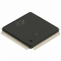
CY7C9689A-AXC Cypress Semiconductor Corp, CY7C9689A-AXC Datasheet - Page 24

CY7C9689A-AXC
Manufacturer Part Number
CY7C9689A-AXC
Description
IC TXRX HOTLINK 100LQFP
Manufacturer
Cypress Semiconductor Corp
Series
CY7Cr
Type
Transceiverr
Datasheet
1.CY7C9689A-AXC.pdf
(51 pages)
Specifications of CY7C9689A-AXC
Package / Case
100-LQFP
Voltage - Supply
4.5 V ~ 5.5 V
Mounting Type
Surface Mount
Product
PHY
Interface Type
Parallel
Supply Voltage (max)
6.5 V
Supply Voltage (min)
2 V
Supply Current
250 mA
Maximum Operating Temperature
+ 70 C
Minimum Operating Temperature
0 C
Mounting Style
SMD/SMT
Number Of Channels
2
Ic Interface Type
Parallel, Serial
Supply Voltage Range
4.5V To 5.5V
Operating Temperature Range
0°C To +70°C
Digital Ic Case Style
TQFP
No. Of Pins
100
Msl
MSL 3 - 168 Hours
No. Of Receivers
2
Rohs Compliant
Yes
Frequency Max
50MHz
Lead Free Status / RoHS Status
Lead free / RoHS Compliant
Number Of Drivers/receivers
-
Protocol
-
Lead Free Status / Rohs Status
Lead free / RoHS Compliant
Available stocks
Company
Part Number
Manufacturer
Quantity
Price
Company:
Part Number:
CY7C9689A-AXC
Manufacturer:
ALTERA
Quantity:
112
Company:
Part Number:
CY7C9689A-AXC
Manufacturer:
CY
Quantity:
86
Company:
Part Number:
CY7C9689A-AXC
Manufacturer:
CYPRESS
Quantity:
273
Company:
Part Number:
CY7C9689A-AXC
Manufacturer:
Cypress Semiconductor Corp
Quantity:
10 000
Part Number:
CY7C9689A-AXC
Manufacturer:
CYPRESS/赛普拉斯
Quantity:
20 000
Document #: 38-02020 Rev. *E
CY7C9689A Transmitter TTL Switching Characteristics, FIFO Enabled
CY7C9689A Receiver TTL Switching Characteristics, FIFO Enabled
f
t
t
t
t
t
t
t
t
t
t
t
t
t
Notes
f
t
t
t
t
t
t
t
t
t
t
t
t
t
t
t
t
t
RIS
RXCLKIP
RXCPWH
RXCPWL
RXCLKIR
RXCLKIF
RXENS
RXENH
RXRSS
RXRSH
RXCES
RXCEH
RXA
RXZA
18. Input/output rise and fall time is measured between 0.8V and 2.0V
19. Parallel data output specifications are only valid if all outputs are loaded with similar DC and AC loads.
TS
TXCLK
TXCPWH
TXCPWL
TXCLKR
TXCLKF
TXA
TXDS
TXDH
TXENS
TXENH
TXRSS
TXRSH
TXCES
TXCEH
TXZA
TXOE
TXAZ
Parameter
Parameter
[16]
[16]
[16]
[16]
RXCLK Clock Cycle Frequency With Receive FIFO Enabled
RXCLK Input Period
RXCLK Input HIGH Time
RXCLK Input LOW Time
RXCLK Input Rise Time
RXCLK Input Fall Time
Receive Enable Set-up Time to RXCLK↑
Receive Enable Hold Time from RXCLK↑
Receive FIFO Reset (RXRXT) Set-up Time to RXCLK↑
Receive FIFO Reset (RXRXT) Hold Time from RXCLK↑
Receive Chip Enable (CE) Set-up Time to RXCLK↑
Receive Chip Enable (CE) Hold Time from RXCLK↑
Flag and Data Access Time From RXCLK↑ to Output
Sample of CE LOW by RXCLK↑, Output High-Z to Active HIGH or LOW,
or Sample of RXEN Asserted by RXCLK↑, Output High-Z to Active HIGH or LOW
TXCLK Clock Cycle Frequency With Transmit FIFO Enabled
TXCLK Period
TXCLK HIGH Time
TXCLK LOW Time
TXCLK Rise Time
TXCLK Fall Time
Flag Access Time From TXCLK↑ to Output
Transmit Data Set-up Time to TXCLK↑
Transmit Data Hold Time from TXCLK↑
Transmit Enable Set-up Time to TXCLK↑
Transmit Enable Hold Time from TXCLK↑
Transmit FIFO Reset (TXRST) Set-up Time to TXCLK↑
Transmit FIFO Reset (TXRST Hold Time from TXCLK↑
Transmit Chip Enable (CE) Set-up Time to TXCLK↑
Transmit Chip Enable (CE) Hold Time from TXCLK↑
Sample of CE LOW by TXCLK↑, Output High-Z to Active HIGH or LOW
Sample of CE LOW by TXCLK↑ to Output Valid
Sample of CE HIGH by TXCLK↑ to Output in High-Z
[18]
[18]
[18]
[18]
Description
Description
[19]
Over the Operating Range
Over the Operating Range
Min.
Min.
6.5
6.5
0.7
0.7
1.5
1.5
6.5
6.5
0.7
0.7
1.5
20
20
2
4
1
4
1
4
1
4
1
0
4
1
4
1
4
1
0
CY7C9689A
Max.
Max.
50
15
20
20
50
15
5
5
5
5
Page 24 of 51
Unit
MHz
Unit
MHz
ns
ns
ns
ns
ns
ns
ns
ns
ns
ns
ns
ns
ns
ns
ns
ns
ns
ns
ns
ns
ns
ns
ns
ns
ns
ns
ns
ns
ns
ns
[+] Feedback


