DS90C032TMX/NOPB National Semiconductor, DS90C032TMX/NOPB Datasheet - Page 7
DS90C032TMX/NOPB
Manufacturer Part Number
DS90C032TMX/NOPB
Description
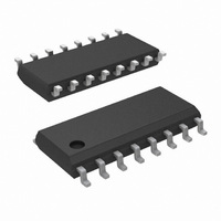
IC LINE RCVR LVDS QUAD 16-SOIC
Manufacturer
National Semiconductor
Type
Receiverr
Datasheet
1.DS90C032TMXNOPB.pdf
(12 pages)
Specifications of DS90C032TMX/NOPB
Number Of Drivers/receivers
0/4
Protocol
RS644
Voltage - Supply
4.5 V ~ 5.5 V
Mounting Type
Surface Mount
Package / Case
16-SOIC (3.9mm Width)
Leaded Process Compatible
Yes
Rohs Compliant
Yes
Peak Reflow Compatible (260 C)
Yes
Lead Free Status / RoHS Status
Lead free / RoHS Compliant
Other names
*DS90C032TMX
DS90C032TMX
DS90C032TMXTR
DS90C032TMX
DS90C032TMXTR
Available stocks
Company
Part Number
Manufacturer
Quantity
Price
Company:

Part Number:
DS90C032TMX/NOPB
Manufacturer:
MAXIM
Quantity:
6 254


3.
4.
the cable is still present and floating, the unplugged cable
can become a floating antenna that can pick up noise.
The LVDS receiver is designed to detect very small
amplitude and width signals and recover them to
standard logic levels. Thus, if the cable picks up more
than 10mV of differential noise, the receiver may
respond. To insure that any noise is seen as common-
mode and not differential, a balanced interconnect and
twisted pair cables is recommended, as they help to
ensure that noise is coupled common to both lines and
rejected by the receivers.
Shorted Inputs. If a fault condition occurs that shorts
the receiver inputs together, thus resulting in a 0V
differential input voltage, the receiver output will remain
in a HIGH state. Shorted input fail-safe is not supported
across the common-mode range of the device (1.2V
±1V). It is only supported with inputs shorted and no
external common-mode voltage applied.
Operation in environment with greater than 10mV
differential noise.
National recommends external failsafe biasing on its
LVDS receivers for a number of system level and signal
7
The footprint of theDS90C032 is the same as the industry
standard 26LS32 Quad Differential (RS-422) Receiver.
quality reasons. First, only an application that requires
failsafe biasing needs to employ it. Second, the amount
of failsafe biasing is now an application design parameter
and can be custom tailored for the specific application. In
applications in low noise environments, they may choose
to use a very small bias if any. For applications with less
balanced interconnects and/or in high noise
environments they may choose to boost failsafe further.
Nationals "LVDS Owner’s Manual provides detailed
calculations for selecting the proper failsafe biasing
resistors. Third, the common-mode voltage is biased by
the resistors during the un-driven state. This is selected
to be close to the nominal driver offset voltage (V
Thus when switching between driven and un-driven
states, the common-mode modulation on the bus is held
to a minimum.
For additional Failsafe Biasing information, please refer
to Application Note AN-1194 for more detail.
www.national.com
OS
).
Related parts for DS90C032TMX/NOPB
Image
Part Number
Description
Manufacturer
Datasheet
Request
R

Part Number:
Description:
IC LINE RCVR LVDS QUAD 16-SOIC
Manufacturer:
National Semiconductor
Datasheet:

Part Number:
Description:
IC, DIFFERENTIAL LINE RECEIVER, SOP-16
Manufacturer:
National Semiconductor
Datasheet:
Part Number:
Description:
National Semiconductor [8-Bit D/A Converter]
Manufacturer:
National Semiconductor
Datasheet:
Part Number:
Description:
National Semiconductor [Media Coprocessor]
Manufacturer:
National Semiconductor
Datasheet:
Part Number:
Description:
Digitally Controlled Tone and Volume Circuit with Stereo Audio Power Amplifier, Microphone Preamp Stage and National 3D Sound
Manufacturer:
National Semiconductor
Datasheet:
Part Number:
Description:
Digitally Controlled Tone and Volume Circuit with Stereo Audio Power Amplifier, Microphone Preamp Stage and National 3D Sound
Manufacturer:
National Semiconductor
Datasheet:
Part Number:
Description:
AC97 Rev 2 Codec with Sample Rate Conversion and National 3D Sound
Manufacturer:
National Semiconductor
Part Number:
Description:
Manufacturer:
National Semiconductor
Datasheet:
Part Number:
Description:
Manufacturer:
National Semiconductor
Datasheet:
Part Number:
Description:
General Purpose, Low Voltage, Low Power, Rail-to-Rail Output Operational Amplifiers
Manufacturer:
National Semiconductor
Datasheet:
Part Number:
Description:
8-bit 20 MSPS flash A/D converter.
Manufacturer:
National Semiconductor
Datasheet:
Part Number:
Description:
Low Noise Quad Operational Amplifier
Manufacturer:
National Semiconductor
Datasheet:
Part Number:
Description:
Quad Differential Line Receivers
Manufacturer:
National Semiconductor
Datasheet:
Part Number:
Description:
Quad High Speed Trapezoidal? Bus Transceiver
Manufacturer:
National Semiconductor
Datasheet: