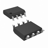
DS90C402M/NOPB National Semiconductor, DS90C402M/NOPB Datasheet - Page 2

DS90C402M/NOPB
Manufacturer Part Number
DS90C402M/NOPB
Description
IC REC LVDS DUAL DIFF SGNL 8SOIC
Manufacturer
National Semiconductor
Type
Receiverr
Datasheet
1.DS90C402MNOPB.pdf
(8 pages)
Specifications of DS90C402M/NOPB
Number Of Drivers/receivers
0/2
Protocol
RS644
Voltage - Supply
4.5 V ~ 5.5 V
Mounting Type
Surface Mount
Package / Case
8-SOIC (3.9mm Width)
Lead Free Status / RoHS Status
Lead free / RoHS Compliant
Other names
*DS90C402M
*DS90C402M/NOPB
DS90C402M
*DS90C402M/NOPB
DS90C402M
Available stocks
Company
Part Number
Manufacturer
Quantity
Price
Company:
Part Number:
DS90C402M/NOPB
Manufacturer:
NSC
Quantity:
650
www.national.com
V
V
I
V
V
I
I
t
t
t
t
t
t
t
Symbol
Symbol
IN
OS
CC
PHLD
PLHD
SKD
SK1
SK2
TLH
THL
TH
TL
OH
OL
Absolute Maximum Ratings
If Military/Aerospace specified devices are required,
please contact the National Semiconductor Sales Office/
Distributors for availability and specifications.
Electrical Characteristics
Over Supply Voltage and Operating Temperature ranges, unless otherwise specified. (Note 2)
Switching Characteristics
V
Supply Voltage (V
Input Voltage (R
Output Voltage (R
Maximum Package Power Dissipation
M Package
Derate M Package
Storage Temperature Range
Lead Temperature Range
CC
Soldering (4 sec.)
= +5.0V
Differential Input High Threshold
Differential Input Low Threshold
Input Current
Output High Voltage
Output Low Voltage
Output Short Circuit Current
No Load Supply Current
Differential Propagation Delay High to Low
Differential Propagation Delay Low to High
Differential Skew |t
Channel-to-Channel Skew (Note 5)
Chip to Chip Skew (Note 6)
Rise Time
Fall Time
±
10%, T
IN+
Parameter
CC
OUT
, R
)
)
A
IN−
= −40˚C to +85˚C (Notes 3, 4, 5, 6, 9)
)
PHLD
− t
Parameter
PLHD
−0.3V to (V
−0.3V to (V
|
@
8.2 mW/˚C above
−65˚C to +150˚C
+25˚C
V
V
V
I
I
I
I
I
V
Inputs Open
OH
OH
OH
OH
OL
CM
IN
IN
OUT
−0.3V to +6V
= 2 mA, V
= +2.4V
= 0V
= −0.4 mA, V
= −0.4mA, Inputs terminated
= −0.4mA, Inputs Open
= −0.4mA, Inputs Shorted
(Note 1)
= + 1.2V
CC
CC
= 0V (Note 8)
1025 mW
+ 0.3V)
+ 0.3V)
+260˚C
+25˚C
ID
V
Conditions
= −200 mV
CC
ID
= +200 mV
2
= 5.5V
Recommended Operating
Conditions
Supply Voltage (V
Receiver Input Voltage
Operating Free Air
Maximum Junction Temperature
ESD Rating (Note 4)
C
V
(Figure 1 and Figure 2)
Temperature (T
(HBM, 1.5 kΩ, 100 pF)
(EIAJ, 0 Ω, 200 pF)
L
ID
= 5 pF,
= 200 mV
Conditions
A
CC
)
)
R
R
R
V
Pin
OUT
IN+
IN−
CC
,
GND
+4.5
Min
−40
−100
Min
Min
−10
−10
−15
1.0
1.0
3.8
3.8
3.8
0
0
+5.0
Typ
+25
3.40
3.48
0.08
0.07
Typ
Typ
−60
±
0.6
0.5
0.5
4.9
4.9
4.9
4.9
3.5
±
1
1
Max
+5.5
+85
2.4
+100
−100
Max
Max
+10
+10
6.0
6.0
1.2
1.5
5.0
2.5
2.5
0.3
10
≥ 3,500V
+150˚C
≥ 250V
Units
˚C
V
V
Units
Units
mV
mV
mA
mA
µA
µA
ns
ns
ns
ns
ns
ns
ns
V
V
V
V
V


