DS90C031TM/NOPB National Semiconductor, DS90C031TM/NOPB Datasheet - Page 4
DS90C031TM/NOPB
Manufacturer Part Number
DS90C031TM/NOPB
Description
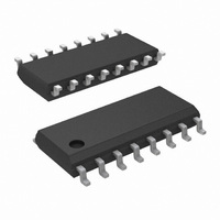
IC LINE DRVR LVDS QUAD 16-SOIC
Manufacturer
National Semiconductor
Type
Driverr
Datasheet
1.DS90C031TMNOPB.pdf
(14 pages)
Specifications of DS90C031TM/NOPB
Number Of Drivers/receivers
4/0
Protocol
LVDS
Voltage - Supply
4.5 V ~ 5.5 V
Mounting Type
Surface Mount
Package / Case
16-SOIC (3.9mm Width)
Supply Current
21mA
Supply Voltage Range
4.5V To 5.5V
Driver Case Style
SOIC
No. Of Pins
16
Operating Temperature Range
-40°C To +85°C
Msl
MSL 1 - Unlimited
Data Rate Max
155.5Mbps
Rohs Compliant
Yes
Lead Free Status / RoHS Status
Lead free / RoHS Compliant
Other names
*DS90C031TM
*DS90C031TM/NOPB
DS90C031TM
*DS90C031TM/NOPB
DS90C031TM
Available stocks
Company
Part Number
Manufacturer
Quantity
Price
Company:

Part Number:
DS90C031TM/NOPB
Manufacturer:
ADI
Quantity:
27


www.national.com
Symbol
t
t
t
t
t
t
Symbol
t
t
t
t
t
t
t
t
t
t
t
Symbol
t
t
t
t
t
t
t
t
t
TLH
THL
PHZ
PLZ
PZH
PZL
PHLD
PLHD
SKD
SK1
SK2
TLH
THL
PHZ
PLZ
PZH
PZL
PHLD
PLHD
SKD
SK1
SK2
PHZ
PLZ
PZH
PZL
Switching Characteristics
V
Switching Characteristics
V
Switching Characteristics
V
Parameter Measurement Information
CC
CC
CC
= +5.0V, T
= +5.0V
= +5.0V
Rise Time
Fall Time
Disable Time High to Z
Disable Time Low to Z
Enable Time Z to High
Enable Time Z to Low
Differential Propagation Delay High to Low
Differential Propagation Delay Low to High
Differential Skew |t
Channel-to-Channel Skew (Note 4)
Chip to Chip Skew (Note 5)
Rise Time
Fall Time
Disable Time High to Z
Disable Time Low to Z
Enable Time Z to High
Enable Time Z to Low
Differential Propagation Delay High to Low
Differential Propagation Delay Low to High
Differential Skew |t
Channel-to-Channel Skew (Note 4)
Chip to Chip Skew (Note 5)
Disable Time High to Z
Disable Time Low to Z
Enable Time Z to High
Enable Time Z to Low
±
±
A
10%, T
10%, T
= +25˚C DS90C031T. (Notes 3, 4, 6, 9)
A
A
= −40˚C to +85˚C DS90C031T. (Notes 3, 4, 5, 6, 9)
= −55˚C to +125˚C DS90C031E. (Notes 3, 4, 5, 6, 9, 10)
Parameter
Parameter
Parameter
PHLD
PHLD
– t
– t
PLHD
PLHD
FIGURE 1. Driver V
|
|
(Continued)
R
C
( Figure 4 and Figure 5 )
R
( Figure 2 and Figure 3 )
R
C
( Figure 4 and Figure 5 )
R
( Figure 3 )
C
each Output and GND
R
C
( Figure 4 and Figure 5 )
OD
L
L
L
L
L
L
L
L
L
4
= 100 ,
= 5 pF
= 100 , C
= 100 ,
= 5 pF
= 100 , C
Connected between
= 100 ,
= 5 pF
and V
Conditions
Conditions
Conditions
OS
Test Circuit
L
L
= 5 pF
= 20 pF
Min
Min
Min
0.5
0.5
0.5
0.5
0
0
0
0
DS011946-3
0.35
0.35
0.35
0.35
0.08
Typ
Typ
Typ
2.5
2.5
2.5
2.5
2.0
2.1
0.3
2.5
2.5
2.5
2.5
2.0
2.1
0.3
2.5
2.5
2.5
2.5
80
Max
Max
Max
900
1.5
1.5
3.5
3.5
1.0
3.0
2.0
2.0
5.0
5.0
3.0
3.0
4.5
10
10
10
10
15
15
15
15
20
20
20
20
Units
Units
Units
ns
ns
ns
ns
ns
ns
ns
ns
ps
ns
ns
ns
ns
ns
ns
ns
ns
ns
ns
ns
ns
ns
ns
ns
ns
ns
Related parts for DS90C031TM/NOPB
Image
Part Number
Description
Manufacturer
Datasheet
Request
R

Part Number:
Description:
National Semiconductor [8-Bit D/A Converter]
Manufacturer:
National Semiconductor
Datasheet:
Part Number:
Description:
National Semiconductor [Media Coprocessor]
Manufacturer:
National Semiconductor
Datasheet:
Part Number:
Description:
Digitally Controlled Tone and Volume Circuit with Stereo Audio Power Amplifier, Microphone Preamp Stage and National 3D Sound
Manufacturer:
National Semiconductor
Datasheet:
Part Number:
Description:
Digitally Controlled Tone and Volume Circuit with Stereo Audio Power Amplifier, Microphone Preamp Stage and National 3D Sound
Manufacturer:
National Semiconductor
Datasheet:
Part Number:
Description:
AC97 Rev 2 Codec with Sample Rate Conversion and National 3D Sound
Manufacturer:
National Semiconductor
Part Number:
Description:
Manufacturer:
National Semiconductor
Datasheet:
Part Number:
Description:
Manufacturer:
National Semiconductor
Datasheet:
Part Number:
Description:
General Purpose, Low Voltage, Low Power, Rail-to-Rail Output Operational Amplifiers
Manufacturer:
National Semiconductor
Datasheet:
Part Number:
Description:
8-bit 20 MSPS flash A/D converter.
Manufacturer:
National Semiconductor
Datasheet:
Part Number:
Description:
Low Noise Quad Operational Amplifier
Manufacturer:
National Semiconductor
Datasheet:
Part Number:
Description:
Quad Differential Line Receivers
Manufacturer:
National Semiconductor
Datasheet:
Part Number:
Description:
Quad High Speed Trapezoidal? Bus Transceiver
Manufacturer:
National Semiconductor
Datasheet: