DS90CF364AMTD/NOPB National Semiconductor, DS90CF364AMTD/NOPB Datasheet - Page 13
DS90CF364AMTD/NOPB
Manufacturer Part Number
DS90CF364AMTD/NOPB
Description
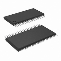
IC RCVR LVDS FPD 18BIT 48-TSSOP
Manufacturer
National Semiconductor
Type
Driverr
Datasheets
1.DS90CF364AMTDNOPB.pdf
(14 pages)
2.DS90CF364MTD.pdf
(16 pages)
3.DS90CF364MTDNOPB.pdf
(16 pages)
Specifications of DS90CF364AMTD/NOPB
Number Of Drivers/receivers
1/0
Protocol
RS644
Voltage - Supply
3 V ~ 3.6 V
Mounting Type
Surface Mount
Package / Case
48-TSSOP
Number Of Drivers
21
Number Of Receivers
3
Data Rate
1300 Mbps
Operating Supply Voltage
3.3 V
Maximum Power Dissipation
1890 mW
Maximum Operating Temperature
+ 70 C
Minimum Operating Temperature
- 10 C
Mounting Style
SMD/SMT
Supply Voltage (max)
3.6 V
Supply Voltage (min)
3 V
Supply Current
60mA
Supply Voltage Range
3V To 3.6V
Driver Case Style
TSSOP
No. Of Pins
48
Operating Temperature Range
-10°C To +70°C
Msl
MSL 2 - 1 Year
Bandwidth
170GHz
Rohs Compliant
Yes
Lead Free Status / RoHS Status
Lead free / RoHS Compliant
Other names
*DS90CF364AMTD
*DS90CF364AMTD/NOPB
DS90CF364AMTD
*DS90CF364AMTD/NOPB
DS90CF364AMTD
Available stocks
Company
Part Number
Manufacturer
Quantity
Price
Company:

Part Number:
DS90CF364AMTD/NOPB
Manufacturer:
TI
Quantity:
106


TxIN
TxOUT+
TxOUT−
FPSHIFT IN
R_FB
RTxCLK OUT+
TxCLK OUT−
PWR DWN
V
GND
PLL V
PLL GND
LVDS V
LVDS GND
RxIN+
RxIN−
RxOUT
RxCLK IN+
RxCLK IN−
FPSHIFT OUT
PWR DWN
V
GND
PLL V
PLL GND
LVDS V
LVDS GND
CC
CC
DS90C363 Pin Descriptions — FPD
Link Transmitter
DS90CF364 Pin Descriptions — FPD
Link Receiver
Pin Name
Pin Name
CC
CC
CC
CC
I/O No
I/O No
O
O
O
O
O
O
I
I
I
I
I
I
I
I
I
I
I
I
I
I
I
I
I
I
I
I
I
21 TTL level input. This includes: 6 Red, 6 Green, 6 Blue, and 3 control lines—FPLINE, FPFRAME and
21 TTL level data outputs. This includes: 6 Red, 6 Green, 6 Blue, and 3 control lines—FPLINE, FPFRAME,
3 Positive LVDS differentiaI data output.
3 Negative LVDS differential data output.
1 TTL Ievel clock input. The falling edge acts as data strobe. Pin name TxCLK IN.
1 Programmable strobe select.
1 Positive LVDS differential clock output.
1 Negative LVDS differential clock output.
1 TTL level input. When asserted (low input) TRI-STATES the outputs, ensuring low current at power down.
3 Power supply pins for TTL inputs.
4 Ground pins for TTL inputs.
1 Power supply pin for PLL.
2 Ground pins for PLL.
1 Power supply pin for LVDS outputs.
3 Ground pins for LVDS outputs.
3 Positive LVDS differentiaI data inputs.
3 Negative LVDS differential data inputs.
1 Positive LVDS differential clock input.
1 Negative LVDS differential clock input.
1 TTL Ievel clock output. The falling edge acts as data strobe. Pin name RxCLK OUT.
1 TTL level input. When asserted (low input) the receiver outputs are low.
4 Power supply pins for TTL outputs.
5 Ground pins for TTL outputs.
1 Power supply for PLL.
2 Ground pin for PLL.
1 Power supply pin for LVDS inputs.
3 Ground pins for LVDS inputs.
.
.
DRDY (also referred to as HSYNC, VSYNC, Data Enable).
DRDY (also referred to as HSYNC, VSYNC, Data Enable).
13
Description
Description
www.national.com
Related parts for DS90CF364AMTD/NOPB
Image
Part Number
Description
Manufacturer
Datasheet
Request
R

Part Number:
Description:
National Semiconductor [8-Bit D/A Converter]
Manufacturer:
National Semiconductor
Datasheet:
Part Number:
Description:
National Semiconductor [Media Coprocessor]
Manufacturer:
National Semiconductor
Datasheet:
Part Number:
Description:
Digitally Controlled Tone and Volume Circuit with Stereo Audio Power Amplifier, Microphone Preamp Stage and National 3D Sound
Manufacturer:
National Semiconductor
Datasheet:
Part Number:
Description:
Digitally Controlled Tone and Volume Circuit with Stereo Audio Power Amplifier, Microphone Preamp Stage and National 3D Sound
Manufacturer:
National Semiconductor
Datasheet:
Part Number:
Description:
AC97 Rev 2 Codec with Sample Rate Conversion and National 3D Sound
Manufacturer:
National Semiconductor
Part Number:
Description:
Manufacturer:
National Semiconductor
Datasheet:
Part Number:
Description:
Manufacturer:
National Semiconductor
Datasheet:
Part Number:
Description:
General Purpose, Low Voltage, Low Power, Rail-to-Rail Output Operational Amplifiers
Manufacturer:
National Semiconductor
Datasheet:
Part Number:
Description:
8-bit 20 MSPS flash A/D converter.
Manufacturer:
National Semiconductor
Datasheet:
Part Number:
Description:
Low Noise Quad Operational Amplifier
Manufacturer:
National Semiconductor
Datasheet:
Part Number:
Description:
Quad Differential Line Receivers
Manufacturer:
National Semiconductor
Datasheet:
Part Number:
Description:
Quad High Speed Trapezoidal? Bus Transceiver
Manufacturer:
National Semiconductor
Datasheet:
Part Number:
Description:
Dual Line Receiver
Manufacturer:
National Semiconductor
Datasheet:
Part Number:
Description:
TTL to 10k ECL Level Translator with Latch
Manufacturer:
National Semiconductor
Datasheet: