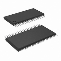
DS90CR216MTD/NOPB National Semiconductor, DS90CR216MTD/NOPB Datasheet - Page 5

DS90CR216MTD/NOPB
Manufacturer Part Number
DS90CR216MTD/NOPB
Description
IC RCVR 21BIT CHAN LINK 48TSSOP
Manufacturer
National Semiconductor
Type
Receiverr
Datasheet
1.DS90CR216MTDNOPB.pdf
(18 pages)
Specifications of DS90CR216MTD/NOPB
Protocol
RS644
Voltage - Supply
3 V ~ 3.6 V
Mounting Type
Surface Mount
Package / Case
48-TSSOP
Lead Free Status / RoHS Status
Lead free / RoHS Compliant
Number Of Drivers/receivers
-
Other names
*DS90CR216MTD
*DS90CR216MTD/NOPB
DS90CR216MTD
*DS90CR216MTD/NOPB
DS90CR216MTD
Available stocks
Company
Part Number
Manufacturer
Quantity
Price
Company:
Part Number:
DS90CR216MTD/NOPB
Manufacturer:
STM
Quantity:
9 000
TPPos5
TPPos6
TCIP
TCIH
TCIL
TSTC
THTC
TCCD
TPLLS
TPDD
CLHT
CHLT
RSPos0
RSPos1
RSPos2
RSPos3
RSPos4
RSPos5
RSPos6
RSPos0
RSPos1
RSPos2
RSPos3
RSPos4
RSPos5
RSPos6
RSKM
RCOP
RCOH
RCOL
RSRC
RHRC
RCCD
RPLLS
RPDD
Symbol
Symbol
Receiver Switching Characteristics
Over recommended operating supply and −40°C to +85°C ranges unless otherwise specified
Note 5: Receiver Skew Margin is defined as the valid data sampling region at the receiver inputs. This margin takes into account for transmitter pulse positions
(min and max) and the receiver input setup and hold time (internal data sampling window). This margin allows LVDS interconnect skew, inter-symbol interference
(both dependent on type/length of cable), and clock jitter less than 250 ps.
Note 6: The min. and max. limits are based on the worst bit by applying a −400ps/+300ps shift from ideal position.
Note 7: The min. and max. are based on the actual bit position of each of the 7 bits within the LVDS data stream across PVT.
Transmitter Output Pulse Position for Bit5
Transmitter Output Pulse Position for Bit6
TxCLK IN Period (Figure 6)
TxCLK IN High Time (Figure 6)
TxCLK IN Low Time (Figure 6)
TxIN Setup to TxCLK IN (Figure 6)
TxIN Hold to TxCLK IN (Figure 6)
TxCLK IN to TxCLK OUT Delay @ 25°C,V
Transmitter Phase Lock Loop Set (Figure 10)
Transmitter Powerdown Delay (Figure 14)
CMOS/TTL Low-to-High Transition Time (Figure 3)
CMOS/TTL High-to-Low Transition Time (Figure 3)
Receiver Input Strobe Position for Bit 0 (Note 7)(Figure 17)
Receiver Input Strobe Position for Bit 1
Receiver Input Strobe Position for Bit 2
Receiver Input Strobe Position for Bit 3
Receiver Input Strobe Position for Bit 4
Receiver Input Strobe Position for Bit 5
Receiver Input Strobe Position for Bit 6
Receiver Input Strobe Position for Bit 0 (Note 6)(Figure 17)
Receiver Input Strobe Position for Bit 1
Receiver Input Strobe Position for Bit 2
Receiver Input Strobe Position for Bit 3
Receiver Input Strobe Position for Bit 4
Receiver Input Strobe Position for Bit 5
Receiver Input Strobe Position for Bit 6
RxIN Skew Margin (Note 5) (Figure 18)
RxCLK OUT Period (Figure 7)
RxCLK OUT High Time (Figure 7)
RxCLK OUT Low Time (Figure 7)
RxOUT Setup to RxCLK OUT (Figure 7)
RxOUT Hold to RxCLK OUT (Figure 7)
RxCLK IN to RxCLK OUT Delay (Figure 9)
Receiver Phase Lock Loop Set (Figure 11)
Receiver Powerdown Delay (Figure 15)
Parameter
Parameter
CC
=3.3V (Figure 8)
5
f = 40 MHz
f = 66 MHz
f = 40 MHz
f = 66 MHz
f = 40 MHz
f = 66 MHz
f = 40 MHz
f = 66 MHz
f = 40 MHz
f = 66 MHz
f = 40 MHz
f = 66 MHz
f = 40 MHz
f = 66 MHz
0.35T
0.35T
10.6
12.8
Min
2.5
15
0
3
0.5T
0.5T
11.0
13.2
Typ
3.7
T
11.6
15.1
18.8
22.5
11.7
13.9
10.0
Min
490
400
1.0
4.5
8.1
0.7
2.9
5.1
7.3
9.5
6.0
4.0
6.0
6.5
2.5
6.0
2.5
4.0
5.0
15
11.9
15.6
19.2
22.9
12.1
14.3
10.0
13.0
14.0
Typ
2.2
2.2
1.4
5.0
8.5
1.1
3.3
5.5
7.7
9.9
6.1
7.8
8.0
8.0
4.0
6.7
6.6
T
0.65T
0.65T
Max
11.3
13.5
100
5.5
50
10
Max
2.15
9.15
12.6
16.3
19.9
23.6
10.2
12.4
14.6
www.national.com
5.0
5.0
5.8
1.4
3.6
5.8
8.0
8.0
9.0
50
10
1
Units
Units
ms
ms
ns
ns
ns
ns
ns
ns
ns
ns
ns
ns
ns
ns
ns
ns
ns
ns
ns
ns
ns
ns
ns
ns
ns
ns
ns
ps
ps
ns
ns
ns
ns
ns
ns
ns
ns
ns
ns
ns
μs


