USB3311C-CP-TR SMSC, USB3311C-CP-TR Datasheet - Page 7
USB3311C-CP-TR
Manufacturer Part Number
USB3311C-CP-TR
Description
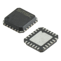
TXRX USB ULPI 26MHZ CLK 24QFN
Manufacturer
SMSC
Series
flexPWR™r
Type
USB Transceiverr
Specifications of USB3311C-CP-TR
Protocol
USB 2.0
Voltage - Supply
1.6 V ~ 3.6 V
Mounting Type
Surface Mount
Package / Case
24-QFN
Operating Supply Voltage
3.3 V
Mounting Style
SMD/SMT
Operating Temperature Range
- 40 C to + 85 C
For Use With
638-1096 - EVALUATION BOARD FOR USB3311C
Number Of Drivers/receivers
-
Lead Free Status / Rohs Status
Lead free / RoHS Compliant
Other names
638-1091-2
USB3311C-CP
USB3311C-CP
Available stocks
Company
Part Number
Manufacturer
Quantity
Price
Company:

Part Number:
USB3311C-CP-TR
Manufacturer:
SMSC
Quantity:
4 000


Hi-Speed USB Transceiver with 1.8V ULPI Interface - 26MHz Reference Clock
SMSC USB3311 REV C
BALL
FLAG
PIN/
C5
B4
B5
A5
A4
A3
B3
B2
A2
A1
C3
15
16
17
18
19
20
21
22
23
24
RESETB
REFCLK
DATA[2]
DATA[1]
DATA[0]
VDD1.8
RBIAS
NAME
GND
NXT
STP
DIR
Table 1 USB3311 Pin Description (continued)
PRODUCT PREVIEW
DIRECTION/
Analog,
Output,
Output,
CMOS,
Ground
CMOS
CMOS
CMOS
CMOS
CMOS
CMOS
CMOS
CMOS
Power
TYPE
Input,
Input,
Input,
I/O,
I/O,
I/O,
7
ACTIVE
LEVEL
High
High
Low
N/A
N/A
N/A
N/A
N/A
N/A
N/A
N/A
ULPI bi-directional data bus.
ULPI bi-directional data bus.
ULPI bi-directional data bus. DATA[0] is
the LSB.
The PHY asserts NXT to throttle the data.
When the Link is sending data to the
PHY, NXT indicates when the current
byte has been accepted by the PHY. The
Link places the next byte on the data bus
in the following clock cycle.
Controls the direction of the data bus.
When the PHY has data to transfer to the
Link, it drives DIR high to take ownership
of the bus. When the PHY has no data to
transfer it drives DIR low and monitors
the bus for commands from the Link.
The Link asserts STP for one clock cycle
to stop the data stream currently on the
bus. If the Link is sending data to the
PHY, STP indicates the last byte of data
was on the bus in the previous cycle.
External 1.8V Supply input pin. This pad
needs to be bypassed with a 0.1uF
capacitor to ground, placed as close as
possible to the USB3311.
When low, the part is suspended with all
of the I/O tri-stated. When high the
USB3311 will operate as a normal ULPI
device.
26MHz Reference Clock input.
Bias Resistor pin. This pin requires an
8.06kΩ (±1%) resistor to ground, placed
as close as possible to the USB3311.
Ground.
QFN only: The flag should be connected
to the ground plane with a via array
under the exposed flag. This is the main
ground for the IC.
DESCRIPTION
Revision 2.1 (06-10-10)
Related parts for USB3311C-CP-TR
Image
Part Number
Description
Manufacturer
Datasheet
Request
R

Part Number:
Description:
Manufacturer:
Standard Microsystems (SMSC)
Datasheet:

Part Number:
Description:
FAST ETHERNET PHYSICAL LAYER DEVICE
Manufacturer:
SMSC Corporation
Datasheet:
Part Number:
Description:
357-036-542-201 CARDEDGE 36POS DL .156 BLK LOPRO
Manufacturer:
SMSC Corporation
Datasheet:
Part Number:
Description:
357-036-542-201 CARDEDGE 36POS DL .156 BLK LOPRO
Manufacturer:
SMSC Corporation
Datasheet:
Part Number:
Description:
357-036-542-201 CARDEDGE 36POS DL .156 BLK LOPRO
Manufacturer:
SMSC Corporation
Datasheet:
Part Number:
Description:
4-PORT USB2.0 HUB CONTROLLER
Manufacturer:
SMSC Corporation
Datasheet:
Part Number:
Description:
Manufacturer:
SMSC Corporation
Datasheet:
Part Number:
Description:
Manufacturer:
SMSC Corporation
Datasheet:
Part Number:
Description:
FDC37C672ENHANCED SUPER I/O CONTROLLER WITH FAST IR
Manufacturer:
SMSC Corporation
Datasheet:
Part Number:
Description:
COM90C66LJPARCNET Controller/Transceiver with AT Interface and On-Chip RAM
Manufacturer:
SMSC Corporation
Datasheet:
Part Number:
Description:
Manufacturer:
SMSC Corporation
Datasheet:
Part Number:
Description:
Manufacturer:
SMSC Corporation
Datasheet:
Part Number:
Description:
Manufacturer:
SMSC Corporation
Datasheet:
Part Number:
Description:
Manufacturer:
SMSC Corporation
Datasheet: