DS26C31TMX/NOPB National Semiconductor, DS26C31TMX/NOPB Datasheet - Page 2
DS26C31TMX/NOPB
Manufacturer Part Number
DS26C31TMX/NOPB
Description
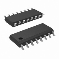
IC LINE DRIVER QUAD CMOS 16-SOIC
Manufacturer
National Semiconductor
Type
Driverr
Datasheet
1.DS26C31TMNOPB.pdf
(13 pages)
Specifications of DS26C31TMX/NOPB
Number Of Drivers/receivers
4/0
Protocol
RS422
Voltage - Supply
4.5 V ~ 5.5 V
Mounting Type
Surface Mount
Package / Case
16-SOIC (3.9mm Width)
Interface Circuit Standard 1
EIA-422/RS-422
Number Of Receivers
Not Required
Number Of Transmitters
4
Number Of Transceivers
Not Required
Data Transmission Topology
Multidrop
Receiver Signal Type
Not Required
Transmitter Signal Type
Differential
Single Supply Voltage (typ)
5V
Single Supply Voltage (min)
4.5V
Single Supply Voltage (max)
5.5V
Dual Supply Voltage (typ)
Not RequiredV
Dual Supply Voltage (min)
Not RequiredV
Dual Supply Voltage (max)
Not RequiredV
Power Supply Requirement
Single
Operating Temp Range
-40C to 85C
Operating Temperature Classification
Industrial
Mounting
Surface Mount
Pin Count
16
Package Type
SOIC N
Leaded Process Compatible
Yes
Rohs Compliant
Yes
Peak Reflow Compatible (260 C)
Yes
Lead Free Status / RoHS Status
Lead free / RoHS Compliant
Other names
DS26C31TMX
DS26C31TMXTR
DS26C31TMXTR
Available stocks
Company
Part Number
Manufacturer
Quantity
Price

Part Number:
DS26C31TMX/NOPB
Manufacturer:
NS/国半
Quantity:
20 000


www.national.com
V
V
V
V
V
|V
V
|V
I
I
I
I
I
IN
CC
OZ
SC
OFF
IH
IL
OH
OL
T
OS
Absolute Maximum Ratings
2)
If Military/Aerospace specified devices are required,
please contact the National Semiconductor Sales Office/
Distributors for availability and specifications.
DC Electrical Characteristics
V
T
OS
Supply Voltage (V
DC Input Voltage (V
DC Output Voltage (V
Clamp Diode Current (I
DC Output Current, per pin (I
DC V
Storage Temperature Range (T
Max. Power Dissipation (P
| − |V
CC
Symbol
per pin (I
Ceramic “J” Pkg.
Plastic “N” Pkg.
− V
= 5V
CC
T
OS
|
or GND Current,
|
±
CC
10% (unless otherwise specified) (Note 4)
)
High Level Input Voltage
Low Level Input Voltage
High Level Output Voltage
Low Level Output
Voltage
Differential Output
Voltage
Difference In
Differential Output
Common Mode
Output Voltage
Difference In
Common Mode Output
Input Current
Quiescent Supply
Current (Note 6)
TRI-STATE Output
Leakage Current
Output Short
Circuit Current
Output Leakage Current
Power Off (Note 5)
CC
IN
)
)
OUT
IK
Parameter
, I
)
D
OK
)
OUT
@
)
25˚C (Note 3)
STG
)
)
−65˚C to +150˚C
−0.5V to 7.0V
−1.5V to V
−0.5V to 7V
(Notes 1,
V
I
V
I
R
(Note 5)
R
(Note 5)
R
(Note 5)
R
(Note 5)
V
DS26C31T
I
DS26C31M
I
V
ENABLE = V
ENABLE = V
V
(Notes 5, 7)
DS26C31T
V
DS26C31M
V
2419 mW
1736 mW
OUT
OUT
OUT
OUT
±
±
IN
IN
IN
OUT
IN
CC
CC
L
L
L
L
±
150 mA
150 mA
= 100Ω
= 100Ω
= 100Ω
= 100Ω
20 mA
= V
= V
= V
= V
+1.5V
= 0V
= 0V
= −20 mA
= 20 mA
= 0 µA
= 0 µA
= V
IH
IH
CC
CC
CC
CC
or V
or V
, GND, V
or GND
or GND
IL
IH
IL
IL
2
Conditions
,
,
V
V
(Note 6)
V
V
(Note 6)
V
V
V
V
(Note 8)
Operating Conditions
IN
IN
IN
IN
OUT
OUT
OUT
OUT
IH
Lead Temperature (T
This device does not meet 2000V ESD Rating. (Note 13)
Supply Voltage (V
DC Input or Output Voltage
Operating Temperature Range (T
Input Rise or Fall Times (t
, or V
= V
= 2.4V or 0.5V
= V
= 2.4V or 0.5V
SOIC “M” Pkg.
Ceramic “W” Pkg.
Ceramic “E” Pkg.
(Soldering, 4 sec.)
(V
DS26C31T
DS26C31M
= 6V
= −0.25V
= 6V
= 0V
IN
CC
CC
, V
IL
or GND
or GND
OUT
)
CC
)
L
)
Min
−30
2.0
2.5
2.0
r
, t
f
)
±
A
Typ
200
200
3.4
0.3
3.1
1.8
0.8
0.8
)
0.5
4.50 5.50
Min Max Units
−40
−55 +125
0
−150
−100
−100
±
±
Max
500
500
100
100
0.8
0.5
0.4
3.0
0.4
2.0
2.1
1.0
5.0
V
+85
500
CC
1226 mW
2134 mW
1182 mW
260˚C
˚C
˚C
ns
Units
V
V
mA
mA
mA
µA
µA
µA
µA
µA
µA
µA
µA
V
V
V
V
V
V
V
V
Related parts for DS26C31TMX/NOPB
Image
Part Number
Description
Manufacturer
Datasheet
Request
R

Part Number:
Description:
IC LINE DRIVER QUAD CMOS 16-SOIC
Manufacturer:
National Semiconductor
Datasheet:

Part Number:
Description:
IC, RS-422 LINE DRIVER, 5.5V, NSOIC-16
Manufacturer:
National Semiconductor
Datasheet:
Part Number:
Description:
National Semiconductor [8-Bit D/A Converter]
Manufacturer:
National Semiconductor
Datasheet:
Part Number:
Description:
National Semiconductor [Media Coprocessor]
Manufacturer:
National Semiconductor
Datasheet:
Part Number:
Description:
Digitally Controlled Tone and Volume Circuit with Stereo Audio Power Amplifier, Microphone Preamp Stage and National 3D Sound
Manufacturer:
National Semiconductor
Datasheet:
Part Number:
Description:
Digitally Controlled Tone and Volume Circuit with Stereo Audio Power Amplifier, Microphone Preamp Stage and National 3D Sound
Manufacturer:
National Semiconductor
Datasheet:
Part Number:
Description:
AC97 Rev 2 Codec with Sample Rate Conversion and National 3D Sound
Manufacturer:
National Semiconductor
Part Number:
Description:
Manufacturer:
National Semiconductor
Datasheet:
Part Number:
Description:
Manufacturer:
National Semiconductor
Datasheet:
Part Number:
Description:
General Purpose, Low Voltage, Low Power, Rail-to-Rail Output Operational Amplifiers
Manufacturer:
National Semiconductor
Datasheet:
Part Number:
Description:
8-bit 20 MSPS flash A/D converter.
Manufacturer:
National Semiconductor
Datasheet:
Part Number:
Description:
Low Noise Quad Operational Amplifier
Manufacturer:
National Semiconductor
Datasheet:
Part Number:
Description:
Quad Differential Line Receivers
Manufacturer:
National Semiconductor
Datasheet:
Part Number:
Description:
Quad High Speed Trapezoidal? Bus Transceiver
Manufacturer:
National Semiconductor
Datasheet: