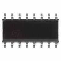
STLVDS050BDR STMicroelectronics, STLVDS050BDR Datasheet

STLVDS050BDR
Specifications of STLVDS050BDR
Available stocks
Related parts for STLVDS050BDR
STLVDS050BDR Summary of contents
Page 1
High speed differential line drivers and receivers Feature summary I Meets or exceed the requirements of ansi eia/tia-644-1995 standard I Signaling rates up to 400Mbit/s I Bus terminal ESD exceeds 6kV I Operates from a single 3.3V supply I Low-voltage ...
Page 2
Contents 1 Pin configuration . . . . . . . . . . . . . . . . . . . . . . . . . . . . . . . . . . . . ...
Page 3
STLVDS050 1 Pin configuration Figure 1. Pin connections and functional diagram Table 1. Pin description Pin n° 1, 10, 11, 13 Table 2. Truth table for receiver V = ...
Page 4
Pin configuration Table 3. Truth table for driver OPEN X L=Low level, H=High Level, X=Don’t care, Z= High Impedance 4/ STLVDS050 ...
Page 5
STLVDS050 2 Maximum ratings Table 4. Absolute maximum ratings Symbol V Supply voltage CC V Voltage range I ESD ESD Protection voltage (HBM) T Storage temperature range STG Note: Absolute Maximum Ratings are those values beyond which damage to the ...
Page 6
Electrical characteristics 3 Electrical characteristics Table 6. Electrical characteristics (Typical values are at T specified). Symbol Parameter I Supply Current CC Table 7. Driver electrical characteristics (Typical values are at T specified). Symbol Parameter Differential output voltage | ...
Page 7
STLVDS050 Table 8. Receiver electrical characteristics (Typical values are at T specified). Symbol Parameter Positive-going differential input V ITH+ voltage threshold Negative-going differential input V ITH- voltage threshold V High level output voltage OH V Low level output voltage OL ...
Page 8
Electrical characteristics Table 10. Receiver switching characteristics (Typical values are at T specified). Symbol Parameter Propagation delay time, low to high t PLH output Propagation delay time, high to low t PHL output t Differential output signal rise time r ...
Page 9
STLVDS050 4 Typical performance characteristics (Unless otherwise specified T Figure 2. Output current vs output high voltage for receiver Figure 4. Output current vs output high voltage for driver Figure 6. High to low propagation delay time for receiver Typical ...
Page 10
Typical performance characteristics Figure 8. High to low propagation delay time for driver 10/15 Figure 9. Low to high propagation delay time for driver STLVDS050 ...
Page 11
STLVDS050 5 Package mechanical data In order to meet environmental requirements, ST offers these devices in ECOPACK packages. These packages have a Lead-free second level interconnect. The category of second Level Interconnect is marked on the package and on the ...
Page 12
Package mechanical data DIM. MIN 0.05 A2 0.8 b 0.19 c 0.09 D 4.9 E 6 0˚ PIN 1 IDENTIFICATION 1 12/15 TSSOP16 MECHANICAL DATA mm. TYP MAX. ...
Page 13
STLVDS050 Tape & Reel TSSOP16 MECHANICAL DATA DIM. MIN 12 6.7 Bo 5.3 Ko 1.6 Po 3.9 P 7.9 mm. TYP MAX. MIN. 330 13.2 0.504 0.795 2.362 22.4 6.9 0.264 5.5 ...
Page 14
Revision history 6 Revision history Table 11. Revision history Date Revision 22-Mar-2006 4 14/15 Order codes has been updated and new template. STLVDS050 Changes ...
Page 15
... STLVDS050 Information in this document is provided solely in connection with ST products. STMicroelectronics NV and its subsidiaries (“ST”) reserve the right to make changes, corrections, modifications or improvements, to this document, and the products and services described herein at any time, without notice. All ST products are sold pursuant to ST’s terms and conditions of sale. ...


