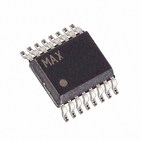
MAX3098EBCEE+ Maxim Integrated Products, MAX3098EBCEE+ Datasheet - Page 11

MAX3098EBCEE+
Manufacturer Part Number
MAX3098EBCEE+
Description
IC RS485/422 RX 32MBPS 16-QSOP
Manufacturer
Maxim Integrated Products
Type
Receiverr
Datasheet
1.MAX3097ECSE.pdf
(16 pages)
Specifications of MAX3098EBCEE+
Number Of Drivers/receivers
0/3
Protocol
RS422, RS485
Voltage - Supply
3 V ~ 5.5 V
Mounting Type
Surface Mount
Package / Case
16-QSOP
Data Rate
32000 Kbps
Propagation Delay Time Ns
75 ns to 85 ns
Operating Supply Voltage
3.3 V to 5.5 V
Supply Current
3.1 mA
Operating Temperature Range
0 C to + 70 C
Input Voltage
3.3 V to 5.5 V
Maximum Power Dissipation
697 mW
Mounting Style
SMD/SMT
Output Current
+/- 105 mA
Output Voltage
- 0.3 V to + 5.3 V
Product
RS-422/RS-485 Combination
Lead Free Status / RoHS Status
Lead free / RoHS Compliant
The MAX3097E/MAX3098E contain circuitry that de-
tects if the input stage is going outside its useful com-
mon-mode range. If the received data could be
unreliable, a fault signal is triggered.
Due to cable attenuation on long wire runs, it is possi-
ble that V
received. In this condition, a fault will be indicated.
The delayed fault output provides a programmable
blanking delay to allow transient faults to occur without
triggering an alarm. Such faults may occur with slow
signals triggering the receiver alarm through the zero
crossover region.
Figure 9 shows the delayed alarm output.
ALARMD performs a logic OR of ALARMA, ALARMB,
and ALARMZ (Figure 10). A NOR gate drives an N-
channel MOSFET so that in normal operation with no
faults, the current source (10µA typ) is shunted to
Triple RS-422/RS-485 Receivers with Fault Detection
Figure 8. Short-Circuit Detection
Figure 9. Delayed Alarm Output
ALARMA
ALARMD
ALARMB
A
A
ID
Detecting Low Input Differential
< 200mV, and incorrect data will be
NORMAL OPERATION
______________________________________________________________________________________
t
D
Common-Mode Range
Delayed Fault Output
±15kV ESD-Protected, 32Mbps, 3V/5V,
SHORT CIRCUIT A TO A
t
D
ground. Upon activation of any alarm from receiver A,
B, or Z, the MOSFET is turned off, allowing the current
source to charge C
DELAY threshold, the comparator output, ALARMD,
goes high. ALARMD is reset when all receiver alarms
go low, quickly discharging C
ALARMD’s delay time is set with a single capacitor
connected from DELAY to GND. The delay comparator
threshold varies with supply voltage, and the C
value can be determined for a given time delay period
from the Capacitance vs. ALARMD Output Delay graph
in the Typical Operating Characteristics or using the
following equations:
and
where t
Figure 10. ALARMD Simplified Schematic
*The capacitor (C
If the duration of an ALARM_ pulse is less than t
output will be present at ALARMD.
ALARMA
ALARMB
ALARMZ
DELAY
ALARM_
ALARMD
t
D
t
D
D
is in µs and C
= 10 + 0.187 x C
= 15 + 0.33 x C
DELAY
) charges up slowly, but discharges rapidly.
DELAY
NMOS
G1
DELAY
DELAY
CURRENT
SOURCE
DELAY
. When V
DELAY
DELAY
is in pF.
(EXTERNAL)
Setting Delay Time
C
DELAY
t
DLY
(for V
(for V
*
DELAY
to ground.
CC
CC
DLY
DELAY THRESHOLD
DELAY
COMPARATOR
= 5V)
, no alarm
= 3V)
exceeds the
ALARMD
DELAY
11


