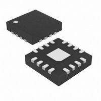
MAX3984UTE+ Maxim Integrated Products, MAX3984UTE+ Datasheet - Page 10

MAX3984UTE+
Manufacturer Part Number
MAX3984UTE+
Description
IC PREMP DRIVER 1CH 16-TQFN
Manufacturer
Maxim Integrated Products
Type
Driverr
Specifications of MAX3984UTE+
Number Of Drivers/receivers
1/0
Protocol
Ethernet
Voltage - Supply
3 V ~ 3.6 V
Mounting Type
Surface Mount
Package / Case
16-TQFN Exposed Pad
Lead Free Status / RoHS Status
Lead free / RoHS Compliant
1Gbps to 10Gbps Preemphasis Driver with
Receive Equalizer
The MAX3984 is composed of a receiver, a driver, and
an LOS detector with selectable threshold. Equalization
is provided in the receiver. Selectable preemphasis
and selectable output amplitude are included in the
transmitter. The MAX3984 also includes transmit dis-
able control for the output.
Data is fed into the MAX3984 through a CML input stage
and a selectable equalization stage. The fixed equalizer
in the receiver corrects for up to 10in of PCB loss on
FR-4 material at 10Gbps. The fixed equalizer can be
bypassed by setting the IN_LEV pin to a logic-low.
10
4, 8, 9, 16
PIN
______________________________________________________________________________________
10
11
12
13
14
15
—
1
2
3
5
6
7
TX_DISABLE
OUT_LEV
IN_LEV
NAME
OUT+
V
OUT-
V
GND
LOS
PE1
PE0
IN+
IN-
EP
CC1
CC2
Detailed Description
Power-Supply Connection for Inputs. Connect to +3.3V.
Positive Data Input, CML. This input is internally terminated with 50 .
Negative Data Input, CML. This input is internally terminated with 50 .
Circuit Ground
Output-Swing Control Input, LVTTL with 20k Internal Pullup. Set to TTL high or open for maximum
output swing, or set to TTL low for reduced swing.
Output Preemphasis Control Input, LVTTL with 10k Internal Pullup. This pin is the most significant
bit of the 2-bit preemphasis control. Set high or open to assert this pin.
Output Preemphasis Control Input, LVTTL with 10k Internal Pullup. This pin is the least significant
bit of the 2-bit preemphasis control. Set high or open to assert this pin.
Negative Data Output, CML. This output is terminated with 50
Positive Data Output, CML. This output is terminated with 50 to V
Power-Supply Connection for Output. Connect to +3.3V.
Transmitter Disable Input, LVTTL with 10k
less than 10mV
Loss-of-Signal Detect, Open-Collector TTL Output. Requires an external pullup
maximum). This output sinks current when the input signal is above the LOS deassert level. To
disable squelch pull LOS to ground.
Receive Equalization Control Input, LVTTL 40k
LOS assert/deassert levels and 10in FR-4 compensation. Set to TTL low for lower LOS assert/deassert
levels and to bypass the FR-4 equalization.
Exposed Pad. For optimal thermal conductivity, this pad must be soldered to the circuit board
ground.
P-P
. Set low for normal operation.
Receiver
The driver includes four-state preemphasis to compen-
sate for up to 10m of 24 AWG, 100Ω balanced cable,
or 30in of FR-4. The OUT_LEV pin selects the output
amplitude. When OUT_LEV is low, the peak-to-peak
amplitude is 1000mV
peak-to-peak amplitude is 1200mV
Input LOS detection is provided. This is an open-collec-
tor output and requires an external pullup resistor
(≥ 4.7kΩ). The pullup resistors should be connected
from LOS to a supply in the +3.0V to +5.5V range. The
LOS output is not valid until power-up is complete.
Internal Pullup. When high or open, differential output is
FUNCTION
Internal Pullup. Set to TTL high or open for higher
to V
P-P
CC2
CC2
. When OUT_LEV is high, the
.
.
Loss of Signal (LOS)
Pin Description
P-P
4.7k
.
(+5.5V
Driver


