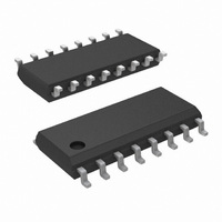
DS34C86TM/NOPB National Semiconductor, DS34C86TM/NOPB Datasheet - Page 3

DS34C86TM/NOPB
Manufacturer Part Number
DS34C86TM/NOPB
Description
IC LINE RCVR QUAD CMOS 16-SOIC
Manufacturer
National Semiconductor
Type
Receiverr
Datasheet
1.DS34C86TMXNOPB.pdf
(8 pages)
Specifications of DS34C86TM/NOPB
Number Of Drivers/receivers
0/4
Protocol
RS422, RS423
Voltage - Supply
4.5 V ~ 5.5 V
Mounting Type
Surface Mount
Package / Case
16-SOIC (3.9mm Width)
Number Of Receivers
4
Number Of Transmitters
Not Required
Number Of Transceivers
Not Required
Data Transmission Topology
Multidrop
Receiver Signal Type
Differential
Transmitter Signal Type
Not Required
Single Supply Voltage (typ)
5V
Single Supply Voltage (min)
4.5V
Single Supply Voltage (max)
5.5V
Dual Supply Voltage (typ)
Not RequiredV
Dual Supply Voltage (min)
Not RequiredV
Dual Supply Voltage (max)
Not RequiredV
Supply Current
23mA
Power Supply Requirement
Single
Operating Temp Range
-40C to 85C
Operating Temperature Classification
Industrial
Mounting
Surface Mount
Pin Count
16
Package Type
SOIC N
Lead Free Status / RoHS Status
Lead free / RoHS Compliant
Other names
*DS34C86TM
DS34C86TM
DS34C86TM
Available stocks
Company
Part Number
Manufacturer
Quantity
Price
t
t
PZL
PZH
t
t
t
t
t
t
PHL(D)
PLH(D)
PLZ
PHZ
PZH
PZL
AC Electrical Characteristics
V
Note 1: Absolute Maximum Ratings are those values beyond which the safety of the device cannot be guaranteed. They are not meant to imply that the device
should be operated at these limits. The table of “Electrical Characteristics” provides conditions for actual device operation.
Note 2: Unless otherwise specified, all voltages are referenced to ground.
Note 3: Unless otherwise specified, Min/Max limits apply across the operating temperature range.
Note 4: ESD Rating; HBM (1.5kΩ, 100 pF)
Note 5: Ratings apply to ambient temperature at 25˚C. Above this temperature derate N Package 13.16 mW/˚C, and M Package 9.52 mW/˚C.
Comparison Table of Switching Characteristics into “LS-Type” Load
V
Note 6: This Table is provided for comparison purposes only. The values in this table for the DS34C86 reflect the performance of the device but are not tested or
guaranteed.
Test and Switching Waveforms
CC
CC
,
All typicals are given for V
Inputs ≥ 2000V
All other pins ≥ 1000V
EIAJ (0Ω, 200 pF) ≥ 350V
Symbol
Symbol
= 5V
= 5V, T
±
10% (unless otherwise specified) (Figures 1, 2, 3)
A
= 25˚C (Figures 4, 5)
Propagation Delay
ENABLE to Output
Propagation Delay Time
Output High to Low
Propagation Delay Time
Output Low to High
Output Low to TRI-STATE
Output High to TRI-STATE
Output TRI-STATE to High
Output TRI-STATE to Low
CC
= 5V and T
Parameter
Parameter
A
= 25˚C.
FIGURE 1. Propagation Delays
V
C
R
V
DIFF
DIFF
(Note 3) (Continued)
L
L
= 50 pF
= 1000Ω
Conditions
= 2.5V
= 2.5V
Typ
17
19
13
12
13
13
3
DS34C86
Max
Min
Typ
19
19
23
25
18
20
00869903
Typ
13
DS3486
Max
Max
21
www.national.com
(Note 6)
Units
Units
ns
ns
ns
ns
ns
ns
ns


